
Page 562 - Design for Six Sigma a Roadmap for Product Development
P. 562
520 Chapter Fourteen
Diode
R 3 R 1 Relay
– 1
E 0 E +
Z
2
R T R 2
R 4
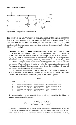
Figure 14.14 Temperature control circuit.
For example, in a power supply circuit design, if the output response
is the output voltage, then we need to find one extreme noise factor
combination which will make output voltage lower, that is, N1, and
another set of noise factor combination which will make output voltage
higher, that is, N2.
Example 14.3. Compounded Noise Factors (Phadke 1989) Figure 14.14
illustrates the circuit diagram of a temperature control circuit, in which R T
is the thermistor resistance, which is inversely proportional to temperature.
R 1 , R 2 , R 3 , and R T actually form a Wheatstone bridge. When temperature
decreases and R T increases, after R T increases to a value R T,on , the
Wheatstone bridge is out of balance and will trigger the amplifier to activate
the heater. After the heater is on for a while, the temperature increases and
R T decreases; after R T decreases to a value R T,off , the amplifier will shut off
the heater and the process will continue.
In a robust parameter design experiment, R T , on is an output response y.
The variation of circuit design parameters R 1 , R 2 , R 4 , E 0 , and E z are noise
factors. The noise factor levels are given in the following table:
Levels
Factor 1 2 3
R 1 2% below nominal value Nominal value 2% above nominal value
R 2 2% below nominal value Nominal value 2% above nominal value
R 4 2% below nominal value Nominal value 2% above nominal value
E 0 2% below nominal value Nominal value 2% above nominal value
E Z 2% below nominal value Nominal value 2% above nominal value
Through standard circuit analysis, R T , on can be expressed by the following
simple mathematical equation:
R 3 R 2 (E Z R 4 E 0 R 1 )
R T,on
R 1 (E Z R 2 E Z R 4 E 0 R 2 )
If we try to design an outer array for noise factors, we may have to use an
L 18 array to accommodate 5 three-level factors, which would be very expen-
sive. So we would like to use compounded noise factors. From the equation,