
Page 874 - Mechanical Engineers' Handbook (Volume 2)
P. 874
2 Microfabrication Procedures 865
Because of the varieties of materials used in MEMS fabrication, the processes for pro-
ducing and modifying them widened far beyond those found in the IC industry. However,
something more fundamental is at work when it comes to processes for making MEMS.
Integrated circuits are monolithic and, despite up to 30 layers in some cases, are made by
largely two-dimensional thin-film processes that yield what some call 2.5-dimensional struc-
tures. By contrast, micromechanical devices must have space between their parts so they can
move, and the dimension perpendicular to the substrate is often very fundamentally necessary
for their performance. Development of processes to make micrometer-scale parts that can
move relative to each other was the breakthrough that enabled MEMS. Such micromachining
processes fall into three major categories, which will now be reviewed briefly.
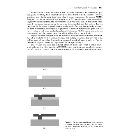
Surface micromachining involves the buildup of micromechanical structures on the sur-
face of a substrate by deposition, patterning, and etching processes. The key step is the
etching away of an earlier deposited and patterned sacrificial layer in order to free the
mechanism. Figure 2 shows the steps needed for such processing. 1,2
This process was first demonstrated about 35 years ago, when a metal–oxide–
semiconductor field effect transistor (MOSFET) with a cantilever mechanical gate was pro-
3
duced. The most common sacrificial material now is silicon dioxide, which is conveniently
(a)
(b)
(c)
Figure 2 Surface micromachining steps: (a) Step
1: Deposit sacrifical layer. (b) Step 2: Pattern layers.
(c) Step 3: Deposit structure layer. (d) Step 4: Etch
(d) sacrifical layer.