
Page 875 - Mechanical Engineers' Handbook (Volume 2)
P. 875
866 Introduction to Microelectromechanical Systems (MEMS): Design and Application
dissolved from under a movable part using hydrofluoric acid. Surface micromachining has
been used to produce an amazing variety of micromechanical devices, some of which are
now in large-scale production. Microaccelerometers and MEMS angle rate sensors are ex-
amples.
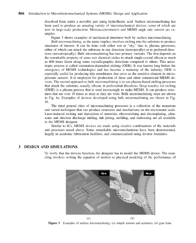
Figure 3 shows examples of mechanical structures built by surface micromachining.
Bulk micromachining, as the name implies, involves etching into the substrate to produce
structures of interest. It can be done with either wet or ‘‘dry,’’ that is, plasma, processes,
either of which can attack the substrate in any direction (isotropically) or in preferred direc-
tions (anisotropically). Bulk micromachining has two primary variants. The first depends on
the remarkable property of some wet chemical etches to attack single-crystal silicon as much
as 600 times faster along some crystallographic directions compared to others. This aniso-
tropic process is called orientation-dependent etching (ODE). It was known long before the
emergence of MEMS technologies and has become a mainstay of the industry. ODE is
especially useful for producing thin membranes that serve as the sensitive element in micro-
pressure sensors. It is employed for production of these and other commercial MEMS de-
vices. The second approach to bulk micromachining is to use plasma-based etching processes
that attack the substrate, usually silicon, in preferential directions. Deep reactive ion etching
(DRIE) is a plasma process that is used increasingly to make MEMS. It can produce struc-
tures that are over 10 times as deep as they are wide. Bulk micromachining steps are shown
in Fig. 4a. Examples of devices developed using bulk micromachining are shown in Fig.
4b.
The third general class of micromachining processes is a collection of the numerous
and varied techniques that can produce structures and mechanisms on the micrometer scale.
Laser-induced etching and deposition of materials, electroetching and electroplating, ultra-
sonic and electron discharge milling, ink jetting, molding, and embossing are all available
to the MEMS designer.
Similar to ICs, MEMS devices are made using creative combinations of the materials
and processes noted above. Some remarkable micromechanisms have been demonstrated,
largely in academic fabrication facilities, and commercialized using diverse foundries.
3 DESIGN AND SIMULATIONS
To verify that the devices function, the designer has to model the MEMS device. The mod-
eling involves writing the equation of motion or physical modeling of the performance of
(a) (b)
Figure 3 Examples of surface micromachining: (a) simple sensors and actuators; (b) gear train.