
Page 877 - Mechanical Engineers' Handbook (Volume 2)
P. 877
868 Introduction to Microelectromechanical Systems (MEMS): Design and Application
incorporates the MEMS design environment into existing and well-known environments with
easy intellectual property (IP) cells or design reuse and the ability to exchange data between
multidisplinary teams. The MEMSCAP simulator is based on the CADENCE environment,
so the designer can simulate MEMS devices with the IC schematics and simulation. Models
can be generated from the ANSYS finite-element model or from written analytical equations.
Behavior models/scalable symbolic view can be generated. The Verilog-A model can also
be generated. The generated model can be used to perform optimization simulations inside
the environment or to realize a system simulation. In addition, emulators are available for
etching, cross section projection of the different material layers.
The design of MEMS devices involves knowledge of the sequence of materials to be
used to realize the device. The sequence of materials used could be the standard sequence,
in which case a standard technology process may be used in conjunction with other proc-
essing steps, for example, postprocessing. The sequence of materials to be used could be
custom designed by the designer, which requires knowledge of the materials and their thin-
film properties. Designers usually design the device and identify the material to be used and
then use CAD tools to verify the performance. Iteration procedures are part of the design
until the required performance is reached. After satisfactory simulation performance, the
device is sent to fabrication foundries.
4 FABRICATION FOUNDRIES
After designing and simulating MEMS and deciding on the materials they will contain and
the processes needed to make them, the next concern is which fabrication facility to employ.
Sometimes, a standard IC facility can be used with postprocessing steps. Postprocessing
involves adding or removing materials from the standard fabricated device. For example,
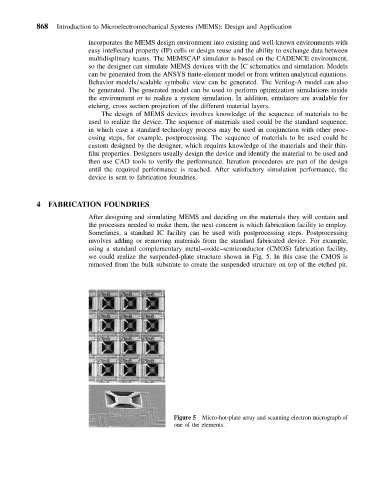
using a standard complementary metal–oxide–semiconductor (CMOS) fabrication facility,
we could realize the suspended-plate structure shown in Fig. 5. In this case the CMOS is
removed from the bulk substrate to create the suspended structure on top of the etched pit.
Figure 5 Micro-hot-plate array and scanning electron micrograph of
one of the elements.