
Page 878 - Mechanical Engineers' Handbook (Volume 2)
P. 878
4 Fabrication Foundries 869
For example, the micro-hot-plate shown in Fig. 5 was realized in CMOS technology in a
standard foundry with a postprocessing step of bulk micromachining to produce the sus-
pended thin film with a resistive heater. The small mass of the heated element permits
temperature changes of 300 C in a few milliseconds.
Many MEMS structures and devices have been produced by such postprocessing of
CMOS chips. 8–10 Techniques which are not compatible with CMOS have also been used, in
which case surface micromachining techniques produce mechanical structures on top of the
substrate. A micromirror fabricated using surface micromachining is an example of such a
device.
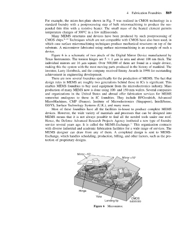
Figure 6 is a schematic of two pixels of the Digital Mirror Device manufactured by
Texas Instruments. The torsion hinges are 5 1 m in area and about 100 nm thick. The
individual mirrors are 16 m square. Over 500,000 of them are found in a single device,
making this the system with the most moving parts produced in the history of mankind. The
inventor, Larry Hornbeck, and the company received Emmy Awards in 1998 for outstanding
achievement in engineering development.
There are now several foundries specifically for the production of MEMS. The fact that
design rules in MEMS are roughly two generations behind those in ICs is significant. This
enables MEMS foundries to buy used equipment from the microelectronics industry. Mass
production of many MEMS now is done using 100- and 150-mm wafers. Several companies
and organizations in the United States and abroad offer fabrication services for MEMS
somewhat analogous to those in IC foundries. They include BFGoodrich, Advanced
MicroMachines, CMP (France), Institute of Microelectronics (Singapore), IntelliSense,
ISSYS, Surface Technology Systems (U.K.), and many more.
Most of these foundries have all the facilities in-house to produce complete MEMS
devices. However, the wide variety of materials and processes that can be designed into
MEMS means that it is not always possible to find all the needed tools under one roof.
Hence, the Defense Advanced Research Projects Agency instituted a new type of foundry
service several years ago. It is called the MEMS-Exchange. 11 This organization contracts
with diverse industrial and academic fabrication facilities for a wide range of services. The
MEMS designer can draw from any of them. A completed design is sent to MEMS-
Exchange, which handles scheduling, production, billing, and other factors, such as the pro-
tection of proprietary designs.
Mirror –10°
Mirror +10°
Hinge
Yoke
CMOS
Landing tip substrate
Figure 6 Micromirror.