
Page 360 - ARM Based Microcontroller Projects Using MBED
P. 360
346 14. ADVANCED PROJECTS
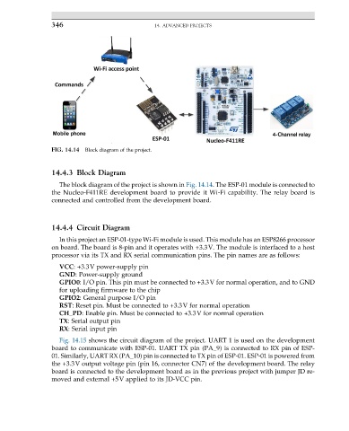
FIG. 14.14 Block diagram of the project.
14.4.3 Block Diagram
The block diagram of the project is shown in Fig. 14.14. The ESP-01 module is connected to
the Nucleo-F411RE development board to provide it Wi-Fi capability. The relay board is
connected and controlled from the development board.
14.4.4 Circuit Diagram
In this project an ESP-01-type Wi-Fi module is used. This module has an ESP8266 processor
on board. The board is 8-pin and it operates with +3.3V. The module is interfaced to a host
processor via its TX and RX serial communication pins. The pin names are as follows:
VCC: +3.3V power-supply pin
GND: Power-supply ground
GPIO0: I/O pin. This pin must be connected to +3.3V for normal operation, and to GND
for uploading firmware to the chip
GPIO2: General purpose I/O pin
RST: Reset pin. Must be connected to +3.3V for normal operation
CH_PD: Enable pin. Must be connected to +3.3V for normal operation
TX: Serial output pin
RX: Serial input pin
Fig. 14.15 shows the circuit diagram of the project. UART 1 is used on the development
board to communicate with ESP-01. UART TX pin (PA_9) is connected to RX pin of ESP-
01. Similarly, UART RX (PA_10) pin is connected to TX pin of ESP-01. ESP-01 is powered from
the +3.3V output voltage pin (pin 16, connector CN7) of the development board. The relay
board is connected to the development board as in the previous project with jumper JD re-
moved and external +5V applied to its JD-VCC pin.