
Page 77 - Alternative Energy Systems in Building Design
P. 77
CRYSTALLINE, AMORPHOUS, THIN-FILM, AND SUN-TRACKER TECHNOLOGIES 53
SEED
SILICON INGOT
QUARTZ CRUCIBLE
WATER COOLED JECKET
HEAT SHIELD
CARBON HEATER
GRAPHITE CRUCIBLE
GRUCIBLE SUPPORT
SPILL TRAY
ELECTRODE
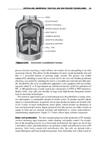
Figure 3.16 Czochralski crystallization furnace.
process involves inserting a metal whisker into molten silicon and pulling it out with
increasing velocity. This allows for the formation of a pure crystal around the wire and
thus is a successful method of growing single crystals. The process was further
enhanced by attaching a small silicon crystal seed to the wire rod. Further production
efficiency was gained by attaching the seed to a rotatable and vertically movable spin-
dle. Incidentally, the same crystallization apparatus is also equipped with special dop-
ing ports where P- or N-type dopants are introduced into the crystal for generation of
PN- or NP-junction-type crystals used in the construction of NPN or PNP transistors,
diodes, LEDs, solar cells, and virtually all large-scale, high-density integrated circuitry
used in electronic technologies.
The chemical vaporization and crystallization process described here is energy-inten-
sive and requires a considerable amount of electric power. To produce purified silicon
ingots at a reasonable price, in general, silicon ingot production plants are located with-
in the vicinity of major hydroelectric power plants, which produce an abundance of
low-cost hydroelectric power. Ingots produced from this process are either circular or
square in form and are cleaned, polished, and distributed to various semiconductor-
manufacturing organizations. Figure 3.17 shows silicon ingot cylinders inspection.
Solar cell production The first manufacturing step in the production of PV modules
involves incoming ingot inspection, wafer cleaning, and quality control. On comple-
tion of the incoming process, in a clean-room environment, the ingots are sliced into
1-mm-thick wafers, and both surfaces are polished, etched, and diffused to form a PN
junction. After being coated with antireflective film, the cells are printed with a
metal-filled paste and fired at high temperature. Each individual cell is then tested for