
Page 303 - MEMS and Microstructures in Aerospace Applications
P. 303
Osiander / MEMS and microstructures in Aerospace applications DK3181_c013 Final Proof page 296 1.9.2005 12:45pm
296 MEMS and Microstructures in Aerospace Applications
each mission to provide a contamination control plan (CCP), which defines the
comprehensive contamination control program that will be implemented in the
mission. Additionally, specific verification plans and requirements must be defined
in the CCP.
Regardless of contamination sensitivity, the implementation of the CCP needs
to be addressed in all mission phases in order to prevent any detrimental contam-
ination damage. Among spacecraft systems, performance of optical and thermal
control is most vulnerable to contamination degradation. A high contamination
sensitivity mission is primarily one which relies on optical sensing, and imaging
or spacecraft or both, which require very strict temperature control, while a low
contamination sensitivity mission is generally one with very insensitive optics and
relatively flexible thermal control requirements. Highly sensitive missions usually
require design and implementation of a strict contamination control program ac-
companied with ongoing monitoring and cleaning procedures.
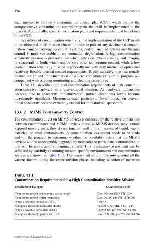
Table 13.1 describes top-level contamination requirements of high contamin-
ation-sensitive hardware in a conventional mission. As hardware dimensions
decrease due to spacecraft miniaturization, surface cleanliness levels become
increasingly significant. Micrometer-sized particles of lesser impact on conven-
tional spacecraft become extremely critical for miniaturized spacecraft.
13.6.2 MEMS CONTAMINATION CONTROL
The contamination effect on MEMS devices is enhanced by the relative dimensions
between contaminants and MEMS devices. Because MEMS devices may contain
exposed moving parts, they do not function well in the presence of liquid, vapor,
particles, or other contaminants. A contamination assessment needs to be made
early in the program to determine whether the possibility exists that the MEMS
devices will be unacceptably degraded by molecular or particulate contaminants, or
if it will be a source of contaminants itself. This preliminary assessment can be
achieved by carefully examining mission-specific environments and contamination
sources are shown in Table 13.2. The assessment should take into account all the
various factors during the entire mission phases including selection of materials
TABLE 13.1
Contamination Requirements for a High Contamination Sensitive Mission
Requirement Category Quantitative Level
Clean room needed (when optics are exposed) Class 100 per FED-STD-209
Clean room needed (other operations) Class 10,000 per FED-STD-209
Optics allowable molecular (EOL) <100 A ˚
Nonoptics allowable molecular (EOL) Level A per MIL-STD-1246
Optics allowable particulate (EOL) <Level 100 per MIL-STD-1246
Nonoptics allowable particulate (EOL) Level 200–300 per MIL-STD-1246
© 2006 by Taylor & Francis Group, LLC