
Page 164 -
P. 164
MEMS Fabrication 3-119
[Krulevitch, 1994]. Below, we will review stress-measuring techniques, starting with the more traditional
ones and subsequently clarifying the problems and opportunities in stress measuring with surface micro-
machined devices.
3.15.4.2 Disk Method
For all practical purposes, only stresses in the x and y directions are of interest in determining overall
thin-film stress, as a film under high stress can only expand or contract by bending the substrate and
deforming it in a vertical direction. Vertical deformations will not induce stresses in a substrate because
it freely moves in that direction. The latter condition enables us to obtain quite accurate stress values by
measuring changes in bow or radius of curvature of a substrate. The residual stresses in thin films are
large, and sensitive optical or capacitive gauges may measure the associated substrate deflections.
The disk method, which is most commonly used, is based on a measurement of the deflection in the
center of the disk substrate (say, a silicon wafer) before and after processing. Because any change in wafer
shape is directly attributable to the stress in the deposited film, it is relatively straightforward to calculate
stress by measuring these changes. Stress in films using this method is found through the Stoney equa-
tion [Hoffman, 1976], relating film stress to substrate curvature, as follows:
1 E T 2
σ (3.54)
R 6(1 v) t
where R measured radius of curvature of the bent substrate, E/(1 ν) biaxial modulus of the substrate,
T thickness of the substrate and t thickness of the applied film [Singer 1992] The underlying assump-
tions include the following:
The disc substrate is thin and has transversely isotropic elastic properties with respect to the film
normal.
The applied film thickness is much less than the substrate thickness.
The film thickness is uniform.
Temperature of the disk substrate/film system is uniform.
The disc substrate/film system is mechanically free.
The disc substrate without film has no bow.
Stress is equi-biaxial and homogeneous over the entire substrate.
Film stress is constant through the film thickness.
For most films on Si, we assume that t T;for example, t/T measures
10 3 for thin films on Si. The
legitimacy of the uniform thickness, homogeneous, and equi-biaxial stress assumptions depends on the
deposition process. Chemical vapor deposition (CVD) is a widely used process, as it produces relatively
uniform films; however, sputter-deposited films can vary considerably over the substrate. In regard to the
assumption of stress uniformity with film thickness, residual stress can vary considerably through the
thickness of the film. Equation (3.54) gives only an average film stress in such cases. In cases where thin
films are deposited onto anisotropic single-crystal substrates, the underlying assumption of a substrate
with transversely isotropic elastic properties with respect to the film normal is not completely justified.
Using single-crystal silicon substrates possessing moderately anisotropic properties such as 100
or 111 oriented wafers (Equation [3.20]) satisfies the transverse isotropy argument. Any curvature
inherent in the substrate must be measured before film deposition and algebraically added to the final
measured radius of curvature. To give an idea of the degree of curvature, 1 µm of thermal oxide may cause
a 30 µm warp of a 4 in silicon wafer, corresponding to a radius of curvature of 41.7 m.
The following companies offer practical disk method-based instruments to measure stress on wafers:
ADE Corp. (Newton, MA, http://www.adesemiconductor.com/applications.shtml#thinstress ), Tropel
(acquired by Corning in 2001) (Fairport, NY, http://www.corning.com/semiconductoroptics/inside_
semiconductor_optics/tropel.asp ), and KLA Tencor Instruments (Mountain View, CA, http://www.
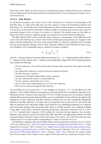
kla-tencor.com/HomePage.asp?version flash [Singer]). Figure 3.84A illustrates the sample output
from Tencor’s optical stress analysis system. Figure 3.84B represents the measuring principle of Ionic
© 2006 by Taylor & Francis Group, LLC