
Page 57 - A Practical Guide from Design Planning to Manufacturing
P. 57
The Evolution of the Microprocessor 33
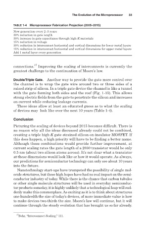
TABLE 1-4 Microprocessor Fabrication Projection (2005–2015)
New generation every 2–3 years
30% reduction in gate length
30% increase in gate capacitance through high-K materials
15% reduction in voltage
30% reduction in interconnect horizontal and vertical dimensions for lower metal layers
15% reduction in interconnect horizontal and vertical dimensions for upper metal layers
Add 1 metal layer every generation
connections. 17 Improving the scaling of interconnects is currently the
greatest challenge to the continuation of Moore’s law.
Double/Triple Gate. Another way to provide the gate more control over
the channel is to wrap the gate wire around two or three sides of a
raised strip of silicon. In a triple gate device the channel is like a tunnel
with the gate forming both sides and the roof (Fig. 1-15). This allows
strong electric fields from the gate to penetrate the silicon and increases
on current while reducing leakage currents.
These ideas allow at least an educated guess as to what the scaling
of devices may look like over the next 10 years (Table 1-4).
Conclusion
Picturing the scaling of devices beyond 2015 becomes difficult. There is
no reason why all the ideas discussed already could not be combined,
creating a triple high-K gate strained silicon-on-insulator MOSFET. If
this does happen, a high priority will have to be finding a better name.
Although these combinations would provide further improvement, at
current scaling rates the gate length of a 2030 transistor would be only
0.5 nm (about two silicon atoms across). It’s not clear what a transistor
at these dimensions would look like or how it would operate. As always,
our predictions for semiconductor technology can only see about 10 years
into the future.
Nanotechnology start-ups have trumpeted the possibility of single mol-
ecule structures, but these high hopes have had no real impact on the semi-
conductor industry of today. While there is the chance that carbon tubules
or other single molecule structures will be used in everyday semiconduc-
tor products someday, it is highly unlikely that a technological leap will sud-
denly make this commonplace. As exciting as it is to think about structures
one-hundredth the size of today’s devices, of more immediate value is how
to make devices two-thirds the size. Moore’s law will continue, but it will
continue through the steady evolution that has brought us so far already.
17
Bohr, “Interconnect Scaling,” 111.