
Page 30 - A Practical Guide from Design Planning to Manufacturing
P. 30
6 Chapter One
column 5 element such as arsenic or phosphorous is added to a silicon
crystal, these atoms will bond with the 4 neighboring silicon atoms leav-
ing one electron left over. This electron is free to move in the conduc-
tion band and acts as a negative carrier. Therefore, adding column 5
elements creates N-type silicon. Column 3 elements, such as boron,
have 3 outer electrons so they naturally create holes in the valence
band, which act as positive charge carriers. Therefore, adding column
3 elements creates P-type silicon. Understanding N-type and P-type
silicon allows us to understand Ohl’s P-N junction diode.
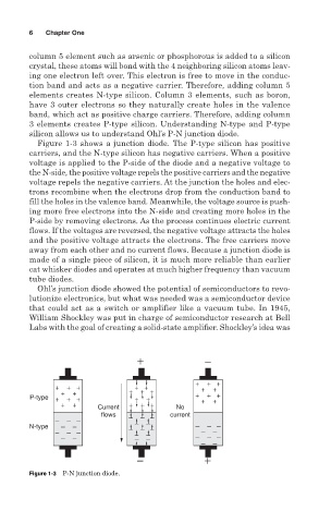
Figure 1-3 shows a junction diode. The P-type silicon has positive
carriers, and the N-type silicon has negative carriers. When a positive
voltage is applied to the P-side of the diode and a negative voltage to
the N-side, the positive voltage repels the positive carriers and the negative
voltage repels the negative carriers. At the junction the holes and elec-
trons recombine when the electrons drop from the conduction band to
fill the holes in the valence band. Meanwhile, the voltage source is push-
ing more free electrons into the N-side and creating more holes in the
P-side by removing electrons. As the process continues electric current
flows. If the voltages are reversed, the negative voltage attracts the holes
and the positive voltage attracts the electrons. The free carriers move
away from each other and no current flows. Because a junction diode is
made of a single piece of silicon, it is much more reliable than earlier
cat whisker diodes and operates at much higher frequency than vacuum
tube diodes.
Ohl’s junction diode showed the potential of semiconductors to revo-
lutionize electronics, but what was needed was a semiconductor device
that could act as a switch or amplifier like a vacuum tube. In 1945,
William Shockley was put in charge of semiconductor research at Bell
Labs with the goal of creating a solid-state amplifier. Shockley’s idea was
+ −
+ + +
+ + + ++ + +
+ + + + +
P-type + + + + + + + + +
+
+ + Current + + + No
flows − − − current
− − − − −
N-type − − − − − − − −
− − − − −
− − − − − − −
−−
− −
− +
Figure 1-3 P-N junction diode.