
Page 145 - Op Amps Design, Applications, and Troubleshooting
P. 145
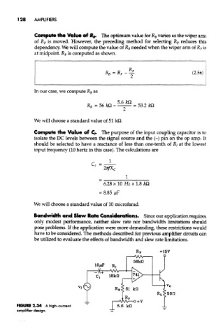
128    AMPLIFIERS


               Compute the Value of &§. The optimum value for R B varies as the wiper arm
               of R P is moved. However, the preceding method for selecting R P reduces this
               dependency. We will compute the value of JR B needed when the wiper arm of R P is
               at midpoint K B is computed as shown.


               In our case, we compute jR B as


               We will choose a standard value of 51 kO.

               Compute the Value of C/. The purpose of the input coupling capacitor is to
               isolate the DC levels between the signal source and the (-) pin on the op amp. It
               should be selected to have a reactance of less than one-tenth of R/ at the lowest
               input frequency (10 hertz in this case). The calculations are


               We will choose a standard value of 10 microfarad.

               Bandwidth and Slew Rate Considerations. Since our application requires
               only modest performance, neither slew rate nor bandwidth limitations should
               pose problems. If the application were more demanding, these restrictions would
               have to be considered. The methods described for previous amplifier circuits can
               be utilized to evaluate the effects of bandwidth and slew rate limitations.