
Page 18 - Power Electronics Handbook
P. 18
- 11
Fabrication process
-
Mass Ion
analyser detector
? -
- - - chamber
- Wafer
Acceleration ’ Beam
ion scanner
source 1
There are several basic requirements which must be met in any
implantation system:
(i) The impurity concentration must be uniform over a given slice, and
the process must be accurately reproducible over repeated slices.
(ii) The system must have a high throughput.
(iii) The punty of the dopant must be accurately controlled. Most ion
sources produce a range of dopants in addition to the one required.
The impurities must be completely removed from the ion stream
before it reaches the silicon slice.
(iv) The energy imparted to the ions by the accelerating voltage must be
high, to enable them to penetrate the maximum distance likely to be
required.
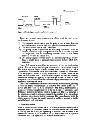
Figure 1.3 shows a simplified arrangement of an ion-implantation
system. The ion source produces an abundance of the required dopant.
The source output should remain constant over a long time, to allow
reproducible devices to be made without the need for constant adjustment.
A focusing system, which is usually electrostatic, is used to focus the ion
beam onto the silicon slice. The ion accelerator gives the ions the neceSgary
penetration energy by applying a high voltage across the ions. A mass
analyser is used in conjunction with the focusing system to separate out the
impurities from the ion beam.
The beam scanner Scans the ion beam over the silicon surface, resulting
in uniform dopant concentration. In addition, the silicon slices can be
moved past the beam for more uniformity. The doping concentration is
monitored by measuring the current in the ion detector. This is quite easily
done since each ion carries one pitive charge unit. The dose imparted to
the silicon, measured in iondcm , is equal to the product of the current and
the exposure time, divided by the wafer area. The wafer chamber holds the
silicon samples. It must be quickly accessible and large enough to hold a
useful batch at each operation.
1.2.7 Metal formation
Metal is deposited onto the surface of the semiconductor slice using one of
two main methods. In the first system the semiconductor is held face down
in the top half of a bell jar, operating in vacuum. The material to be
deposited is located at the bottom of the jar and heated until it vaporim
and settles as a thin layer onto the semiconductor surface.