
Page 139 - Programming Microcontrollers in C
P. 139
124 Chapter 3 What Are Microcontrollers?
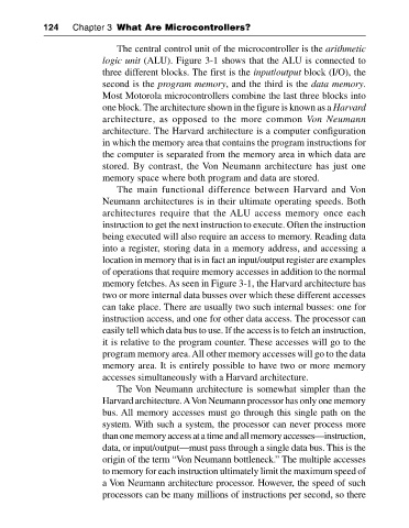
The central control unit of the microcontroller is the arithmetic
logic unit (ALU). Figure 3-1 shows that the ALU is connected to
three different blocks. The first is the input/output block (I/O), the
second is the program memory, and the third is the data memory.
Most Motorola microcontrollers combine the last three blocks into
one block. The architecture shown in the figure is known as a Harvard
architecture, as opposed to the more common Von Neumann
architecture. The Harvard architecture is a computer configuration
in which the memory area that contains the program instructions for
the computer is separated from the memory area in which data are
stored. By contrast, the Von Neumann architecture has just one
memory space where both program and data are stored.
The main functional difference between Harvard and Von
Neumann architectures is in their ultimate operating speeds. Both
architectures require that the ALU access memory once each
instruction to get the next instruction to execute. Often the instruction
being executed will also require an access to memory. Reading data
into a register, storing data in a memory address, and accessing a
location in memory that is in fact an input/output register are examples
of operations that require memory accesses in addition to the normal
memory fetches. As seen in Figure 3-1, the Harvard architecture has
two or more internal data busses over which these different accesses
can take place. There are usually two such internal busses: one for
instruction access, and one for other data access. The processor can
easily tell which data bus to use. If the access is to fetch an instruction,
it is relative to the program counter. These accesses will go to the
program memory area. All other memory accesses will go to the data
memory area. It is entirely possible to have two or more memory
accesses simultaneously with a Harvard architecture.
The Von Neumann architecture is somewhat simpler than the
Harvard architecture. A Von Neumann processor has only one memory
bus. All memory accesses must go through this single path on the
system. With such a system, the processor can never process more
than one memory access at a time and all memory accesses—instruction,
data, or input/output—must pass through a single data bus. This is the
origin of the term “Von Neumann bottleneck.” The multiple accesses
to memory for each instruction ultimately limit the maximum speed of
a Von Neumann architecture processor. However, the speed of such
processors can be many millions of instructions per second, so there