
Page 14 - Science at the nanoscale
P. 14
15:10
RPS: PSP0007 - Science-at-Nanoscale
June 9, 2009
Introduction and Historical Perspective
4
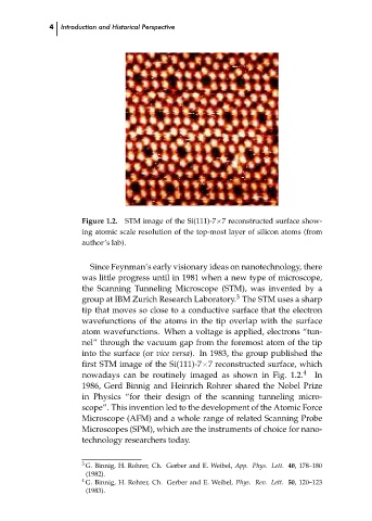
Figure 1.2. STM image of the Si(111)-7×7 reconstructed surface show-
ing atomic scale resolution of the top-most layer of silicon atoms (from
author’s lab).
Since Feynman’s early visionary ideas on nanotechnology, there
was little progress until in 1981 when a new type of microscope,
the Scanning Tunneling Microscope (STM), was invented by a
3
group at IBM Zurich Research Laboratory. The STM uses a sharp
tip that moves so close to a conductive surface that the electron
wavefunctions of the atoms in the tip overlap with the surface
atom wavefunctions. When a voltage is applied, electrons “tun-
nel” through the vacuum gap from the foremost atom of the tip
into the surface (or vice versa). In 1983, the group published the
first STM image of the Si(111)-7×7 reconstructed surface, which ch01
nowadays can be routinely imaged as shown in Fig. 1.2. 4 In
1986, Gerd Binnig and Heinrich Rohrer shared the Nobel Prize
in Physics “for their design of the scanning tunneling micro-
scope”. This invention led to the development of the Atomic Force
Microscope (AFM) and a whole range of related Scanning Probe
Microscopes (SPM), which are the instruments of choice for nano-
technology researchers today.
3 G. Binnig, H. Rohrer, Ch. Gerber and E. Weibel, App. Phys. Lett. 40, 178–180
(1982).
4 G. Binnig, H. Rohrer, Ch. Gerber and E. Weibel, Phys. Rev. Lett. 50, 120–123
(1983).