
Page 53 - Solar Power in Building Design The Engineer's Complete Design Resource
P. 53
CRYSTALLINE SOLAR PHOTOVOLTAIC MODULE PRODUCTION 23
high-temperature vaporization conditions which yielded pure silicon through the
following chemical reaction:
SiCl + 2(Zn) = Si + 2 ZnCl 2
4
The main problem of this process was that SiCl always contained boron chloride
4
(BCl ) when combined with zinc-produced boron, which is a serious contaminant. In
3
1943 a chemical vapor deposition was developed that involved replacement of the zinc
by hydrogen (H), which gave rise to pure silicon since hydrogen, unlike zinc, does not
reduce the boron chloride to boron. Further refinement involved replacement of sili-
con tetrachloride with trichlorosilane (SiHCl ), which is readily reduced to silicon.
3
Czochralski crystal growth In 1916 a Polish metallurgist, Jan Czochralski, devel-
oped a technique to produce silicon crystallization which bears his name. The crystal-
lization process involved inserting a metal whisker into molten silicon and pulling it out
with increasing velocity. This allowed for formation of pure crystal around the wire and
was thus a successful method of growing single crystals. The process was further
enhanced by attaching a small silicon crystal seed to the wire rod. Further production
efficiency was developed by attaching the seed to a rotatable and vertically movable
spindle. Incidentally the same crystallization processing apparatus is also equipped with
special doping ports where P- or N-type dopants are introduced into the crystal for
generation of PN- or NP-junction-type crystals (discussed in Chapter 1), used in the con-
struction of NPN or PNP transistors, diodes, light-emitting diodes, solar cells, and
virtually all high-density, large-scale integrated circuitry used in electronic technologies.
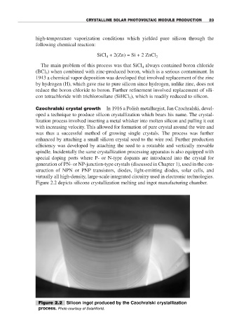
Figure 2.2 depicts silicone crystallization melting and ingot manufacturing chamber.
Figure 2.2 Silicon ingot produced by the Czochralski crystallization
process. Photo courtesy of SolarWorld.