
Page 322 - ARM Based Microcontroller Projects Using MBED
P. 322
308 11. I C BUS PROJECTS
2
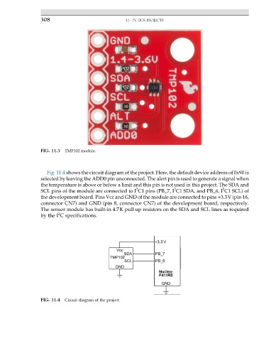
FIG. 11.3 TMP102 module.
Fig. 11.4 shows the circuit diagram of the project. Here, the default device address of 0x90 is
selected by leaving the ADD0 pin unconnected. The alert pin is used to generate a signal when
the temperature is above or below a limit and this pin is not used in this project. The SDA and
2
2
2
SCL pins of the module are connected to I C1 pins (PB_7, I C1 SDA, and PB_6, I C1 SCL) of
the development board. Pins Vcc and GND of the module are connected to pins +3.3V (pin 16,
connector CN7) and GND (pin 8, connector CN7) of the development board, respectively.
The sensor module has built-in 4.7K pull up resistors on the SDA and SCL lines as required
2
by the I C specifications.
FIG. 11.4 Circuit diagram of the project.