
Page 351 - ARM Based Microcontroller Projects Using MBED
P. 351
14.3 PROJECT 1—ANDROID—NUCLEO BOARD COMMUNICATION USING THE WI-FI EXPANSION BOARD 337
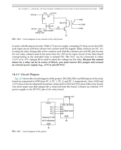
FIG. 14.4 Circuit diagram of one channel of the relay board.
in series with the input circuitry. With a 5V power supply, assuming 2V drop across the LED,
each input circuit will draw about 3mA current from the supply. Relay contacts are NC. Ac-
tivating the relay changes the active contacts such that the common pin and NC pin become
the two relay contacts and at the same time the LED at the input circuit of the relay board
corresponding to the activated relay is turned ON. The VCC can be connected to either
+3.3V or to +5V. Jumper JD is used to select the voltage for the relay. Because the current
drawn by a relay can be in excess of 80mA, you must remove this jumper and connect
an external power supply (e.g., +5V) to pin JD-VCC.
14.3.7 Circuit Diagram
Fig. 14.5 shows the circuit diagram of the project. IN1, IN2, IN3, and IN4 inputs of the relay
board are connected to GPIO pins PC_0, PC_1, PC_2, and PC_3, respectively. Also, GND and
+3.3V pins of the development board are connected to GND and VCC pins of the relay board.
You must make sure that jumper JD is removed from the board. Connect an external +5V
power supply to the JD-VCC pin of the relay board.
FIG. 14.5 Circuit diagram of the project.