
Page 88 - Analog Circuit Design Art, Science, and Personalities
P. 88
Bob Pease
time for a couple years, and a lot of the company’s resources. trying to get the P7
working.
All this experimentation was going on at George A. Philbrick Researches, first at
230 Congress Street and then at 127/129 Clarendon Street, and then at 22 1 Colum-
bus Avenue and 285 Columbus Avenue, in Boston. Massachusetts, back about 32
years ago. George had started a business to sell analog computers, but even in the
1960 era, the business in operational amplifiers (such as the K2-W) was starting to
grow and overshadow the analog computer business. Imagine that-people actually
buying op amps so they could build their own instruments!
When Bob Malter arrived at Philbrick in 1957, he was already a smart and
accomplished engineer. He was a native of Chicago, and he had served in the army
at Dugway Proving Ground. After designing several analog computer modules
(which were the flagships of the Philbrick catalog), he became intrigued with the
concept of the varactor amplifier, about the time that George was getting frustrated.
Now, Bob Malter was a very pragmatic, hard-headed engineer. You would not want
to bet him that he could not do something, because he would determinedly go out
and do it, and prove that he was right-that you were wrong. Bob had his own ideas
on how to simplify the P7, down to a level that would be practical. I do not know
how many false starts and wild experiments Bob made on what he called the P2, but
when I arrived at Philbrick as a green kid engineer in 1960, Bob was just getting the
P2 into production.
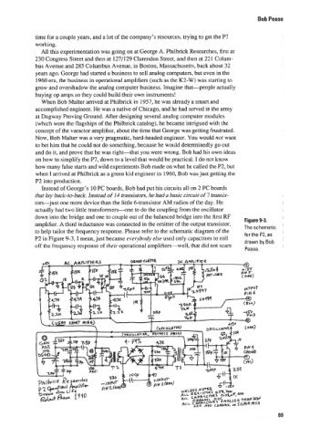
Instead of George’s 10 PC boards, Bob had put his circuits all on 2 PC boards
that lay back-to-back. Instead of 14 transistors, he had a basic circuit of 7 transis-
tors--just one more device than the little 6-transistor AM radios of the day. He
actually had two little transformers-one to do the coupling from the oscillator
down into the bridge and one to couple out of the balanced bridge into the first RF
Figure 9-3.
amplifier. A third inductance was connected in the emitter of the output transistor. The schematic
to help tailor the frequency response. Please refer to the schematic diagram of the for the P2, as
P2 in Figure 9-3. I mean, just because everybody eke used only capacitors tc roll
off the frequency response of their operational amplifiers-well, that did not scare drawn by Bob
Pease.