
Page 83 - Analog Circuit Design Art, Science, and Personalities
P. 83
True Analog Circuit Design
The transition
pulse generator
-HIGH
cs2 cs3
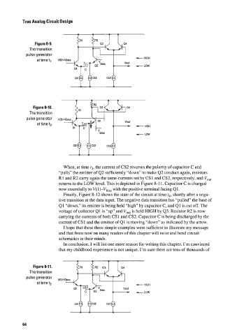
Figure 8-10.
The transition
pulse generator V(+.Vbias * -
at time t2. -
HIGH
Low
When, at time r3, the current of CS2 reverses the polarity of capacitor C and
“pulls” the emitter of 42 sufficiently “down” to make 42 conduct again, resistors
R1 and R2 carry again the same currents set by CS1 and CS2, respectively, and V,,,
returns to the LOW level. This is depicted in Figure 8-1 1. Capacitor C is charged
now essentially to V( 1)-Vbias with the positive terminal facing Q1.
Finally, Figure 8-12 shows the state ofthe circuit at time t4, shortly after a nega-
tive transition at the data input. The negative data transition has “pulled” the base of
Q1 “down,” its emitter is being held “high” by capacitor C, and Q1 is cut off. The
voltage of collector Q1 is “up” and V,,, is held HIGH by 43. Resistor R2 is now
carrying the currents of both CS1 and CS2. Capacitor C is being discharged by the
current of CS I and the emitter of Q 1 is moving “down” as indicated by the arrow.
I hope that these three simple examples were sufficient to illustrate my message
and that from now on many readers of this chapter will twist and bend circuit
schematics in their minds.
In conclusion, I will list one more reason for writing this chapter. I’m convinced
that my childhood experience is not unique. I’m sure there are tens of thousands of
Figure 8-1 1.
The transition
pulse generator
- -HIGH
at time t3
-LOW
-Q Qcs2
64