
Page 80 - Analog Circuit Design Art, Science, and Personalities
P. 80
Tom Hornak
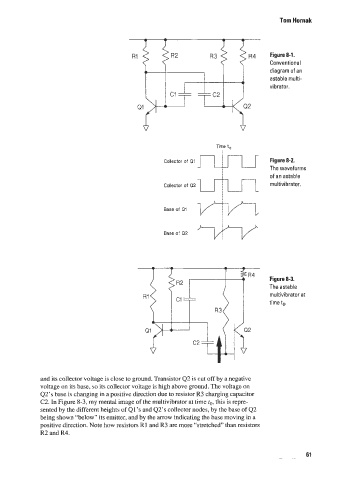
Figure 8-1.
Conventional
diagram of an
astable multi-
vi brator.
Time t,
Collector of Q1 - IJ1J Figure 8-2.
The waveforms
of an astable
Collector of Q2 rnultivibrator.
Base of Q1 l/p/lv
Base 0: Q2
Figure 8-3.
The astable
multivibrator at
time tw
and its collector voltage is close to ground. Transistor Q2 is cut off by a negativc
voltage on its base, so its collector voltage is high abo\/e ground. The voltage on
Q2’s base is changing in a positive direction due to resistor R3 charging capacitor
C2. In Figure 8-3. my mental image of the multivibrator at time to, this is repre-
sented hy the different heights of Q1 ’s and Q2’s collector nodes. by the base of Q2
being shown “below” its emitter, and by the arrow indicating the base moving in a
positive direction. Note how resistors R1 and R3 arc more “stretched” than resistors
R2 and K4.
61