
Page 82 - Analog Circuit Design Art, Science, and Personalities
P. 82
Tom Horeak
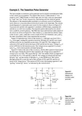
Example 3. The Transition Pulse Generator
The last example is a transition pulse generator used in digital communication links
in their clock recovery portion. The input of the circuit is a data stream in “non-
return-to-zero” (NRZ) format, in which logic ones and logic zeros are represented
by “high” and “low” levels, respectively, each lasting over the whole bit period.
The purpose of the transition pulse generator is Lo generate a pulse of uniform po-
larity whenever a transition from level to level occurs in the input data. The conven-
tional diagram ofa commonly used circuit for this purpose is shown in Figure 8-7.
Transistors Q1 and 42 with capacitor C constitute a differentiator, transistors Q3
and Q4 act as a Full-wave rectifier. The transition pulses delivered by this circuit
have a uniform, positive polarity. The NRZ data input and transition pulse output of
the circuit are shown in Figure 8-8. Time instants l,-t4 represent four distinct states
in the circuit: t, and I; when the circuit is ready for the next transition, and t2 and t4
the state immediately after a data transition has occurred.
Figure 8-9 represents my vision of the circuit at tl, with logic zero level V(0) <
Vbias at its input, waiting for a positive transition. Resistors R1 and R2 carry equal
currents set by the two matched current sinks, CS 1 and CS2. The voltage on the
collectors of Q 1 and Q2 and on the bases of 43 and Q4 are the same. Voltage V,,, is
at the LOW level of the transition pulse. The voltage across capacitor C is essen-
tially Vbi,,-V(0) with its positive terminal facing Q2.
Figure 8- 10 shows the state of the circuit at t2, shortly after a positive transition at
the data input. During the positive data transition, the voltage across capacitor C
changes only very little. This means that Q1 “lifts” the emitter ofQ2 via capacitor C
esscnrially by G’( l)--V(O) and 42 is shut off. The voltage at collector 42 and base
Q4 goes “up,” and the emitter of 44 takes Vou, to the HIGH level. The current
through resistor R1 is now the sum of the currents of CS 1 and CS2. and the col-
lector of Q1 “drops down.’‘ The current of CS2 is now discharging capacitor C and
“pulling” emitter Q2 “down.” as indicated by the vertical arrow.
Figure 8-7.
Conventional
diagram of a
‘transition pulse
generator.
1 Figure 8-8.
Input and output
.
.. . . . .
..
..
TRANSITION ~ ;* f it4 j HIGH signals of the
transition pulse
PULSES
LOW generator.
63