Page 285 - Analog and Digital Filter Design
P. 285

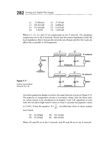
282 Analog and Digital Filter Design


                             L1    27.849mH       C1  77.357nF
                             L2  320.325mH        C2  0.8898pF
                             L3  111.628mH        C3  0.3101yF
                             LA     1.284H        C4  3.5667pF

                       Where L1,  C1, L2, and  C2 are components in the P network. The remaining
                                                     - -
                       components are in the N network. Notice that the source impedance is half  the
                       load impedance, this is because the networks are all-pass and the two loads are
                       effectively in parallel at all frequencies.


                                                           L1
                                                                         L2
                                     Common B                  Common             Pnetwork
                                                                    -
                                                                                    60Ol-l
                                                d&
                                                I  .I


                 Figure 9.17                              tc3 Common t""         N  network
                 Passive Quadrature                                               PO0*
                 Network (N = 4)


                       An active quadrature design to achieve the same function is given in Figure 9.18.
                       The majority of components are set to convenient values, only the shunt resis-
                       tor values remain to be calculated (to be honest I tried  1 nF capacitors to start
                       with, but this led to high resistor values so I had to increase the capacitor values
                                                       1
                       to 2.2nF). Using the equation  R = -,   the following values of  shunt resistor
                                                      OC
                       were found:

                             R1  lO.548kQ        R2  101.335kQ
                             R3  42.283kQ        R4  486.358kQ

                       Where R1 and R2 are in the P network, and R3 and R4 are in the N network.
   280   281   282   283   284   285   286   287   288   289   290