
Page 93 - Applied Photovoltaics
P. 93
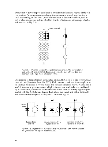
Dissipation of power in poor cells leads to breakdown in localised regions of the cell
                     p-n junction. An enormous power dissipation can occur in a small area, leading to
                     local overheating, or ‘hot spots’, which in turn leads to destructive effects, such as
                     cell or glass cracking or melting of solder. Similar effects occur with groups of cells,
                     as illustrated in Fig. 5.11.

                                                +     open-circuit  +


                                                –                   –

                            Figure 5.11. Potential source of ‘hot spots’ in groups of cells. The combination of
                            cells on the left acts similarly to three series-connected cells with one ‘bad’ cell,
                            as shown on the right (Ross & Smokler, 1986).


                     One solution to the problem of mismatched cells and hot spots is to add bypass diodes
                     to the circuit (Standards Australia, 2005). Under normal conditions, for example, with
                     no shading, each diode is reverse biased and each cell generates power. When a cell is
                     shaded it ceases to generate, acts as a high resistance and tends to be reverse-biased
                     by the other cells, causing the diode across the cell to conduct, thereby bypassing the
                     shaded cell. Fig. 5.12 shows a bypass diode alone, in a circuit and with a faulty cell.
                     The effect on array output of a faulty cell is shown in Fig. 5.13.


                                                          I                    I
                           bypass        cell                   I L                  I L
                            diode                 0                    I – I L

                                                                              0
                                                         I – I L


                                bypass diode     equivalent circuit, I < I L  equivalent circuit, I > I L
                                  and cell         bypass diode off   bypass diode conducts

                            Figure 5.12. A bypass diode in parallel with a cell. When the total current exceeds
                            the I L of this cell, the bypass diode conducts.


                     80