
Page 50 - Bebop to The Boolean Boogie An Unconventional Guide to Electronics Fundamentals, Components, and Processes
P. 50
Semiconductors: Diodes and Transistors 3 1
drain I drain drain I drain
Silicon Silicon
Symbol % mbol
“I
insulator’ insulator’
I source source I source 5ource
(a) NMOS Field-Effect Transistor (b) PMO5 Field-Effect Transistor
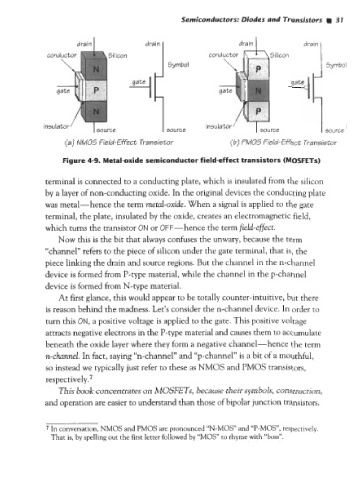
Figure 4-9. Metal-oxide semiconductor field-effect transistors (MOSFETs)
terminal is connected to a conducting plate, which is insulated from the silicon
by a layer of non-conducting oxide. In the original devices the conducting plate
was metal-hence the term metal-oxide. When a signal is applied to the gate
terminal, the plate, insulated by the oxide, creates an electromagnetic field,
which turns the transistor ON or OFF-hence the term field-effect.
Now this is the bit that always confuses the unwary, because the term
“channel” refers to the piece of silicon under the gate terminal, that is, the
piece linking the drain and source regions. But the channel in the n-channel
device is formed from P-type material, while the channel in the p-channel
device is formed from N-type material.
At first glance, this would appear to be totally counter-intuitive, but there
is reason behind the madness. Let’s consider the n-channel device. In order to
turn this ON, a positive voltage is applied to the gate. This positive voltage
attracts negative electrons in the P-type material and causes them to accumulate
beneath the oxide layer where they form a negative channel- hence the term
n-channel. In fact, saying “n-channel” and “p-channel” is a bit of a mouthful,
so instead we typically just refer to these as NMOS and PMOS transistors,
respectively .7
This book concentrates on MOSFETs, because their symbols, construction,
and operation are easier to understand than those of bipolar junction transistors.
7 In conversation, NMOS and PMOS are pronounced “N-MOS” and “P-MOS”, respectively.
That is, by spelling out the first letter followed by “MOS” to rhyme with “boss”.