
Page 330 - Complete Wireless Design
P. 330
Mixer Design
Mixer Design 329
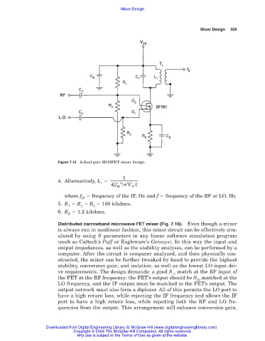
Figure 7.15 A dual-gate MOSFET mixer design.
1
4. Alternatively, L
1 2 2
4[f ( C )]
IF T
where f frequency of the IF, Hz and f frequency of the RF or LO, Hz.
IF
5. R R R 100 kilohms.
1 2 3
6. R 1.2 kilohms.
E
Distributed narrowband microwave FET mixer (Fig. 7.16). Even though a mixer
is always run in nonlinear fashion, this mixer circuit can be effectively sim-
ulated by using S parameters in any linear software simulation program
(such as Caltech’s Puff or Eagleware’s Genesys). In this way the input and
output impedances, as well as the stability analyses, can be performed by a
computer. After the circuit is computer analyzed, and then physically con-
structed, the mixer can be further tweaked by hand to provide the highest
stability, conversion gain, and isolation, as well as the lowest LO input dri-
ve requirements. The design demands: a good S match at the RF input of
11
the FET at the RF frequency; the FET’s output should be S matched at the
22
LO frequency, and the IF output must be matched to the FET’s output. The
output network must also form a diplexer. All of this permits the LO port to
have a high return loss, while rejecting the IF frequency and allows the IF
port to have a high return loss, while rejecting both the RF and LO fre-
quencies from the output. This arrangement will enhance conversion gain,
Downloaded from Digital Engineering Library @ McGraw-Hill (www.digitalengineeringlibrary.com)
Copyright © 2004 The McGraw-Hill Companies. All rights reserved.
Any use is subject to the Terms of Use as given at the website.