
Page 403 - Complete Wireless Design
P. 403
Communications System Design
402 Chapter Nine
and frequency variations so as not to adversely affect the BER of a
phase/amplitude-modulated digital signal.
After all specifications and requirements have been plotted for the commu-
nications system, a detailed block diagram showing the gain, frequency, band-
width, and signal levels (in dBm) should be drawn for the receiver at both its
highest expected input signal level (to confirm that no section is being over-
driven), and its lowest expected input signal level (to confirm that the output
power into the detector is adequate); as well as for the transmitter section.
These diagrams assist in verifying that the gain and bandwidth distribution is
appropriate and that spurious and harmonic suppression will be effective.
After this is accomplished, the actual circuit design for each stage can begin.
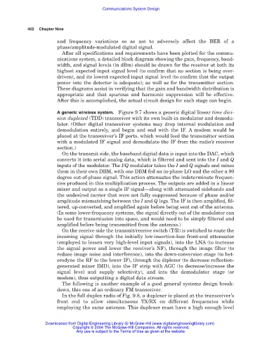
A generic wireless system. Figure 9.7 shows a generic digital linear time divi-
sion duplexed (TDD) transceiver with its own built-in modulator and demodu-
lator. (Other digital transceiver systems may drop internal modulation and
demodulation entirely, and begin and end with the IF. A modem would be
placed at the transceiver’s IF ports, which would feed the transmitter section
with a modulated IF signal and demodulate the IF from the radio’s receiver
section.)
On the transmit side, the baseband digital data is input into the DAC, which
converts it into serial analog data, which is filtered and sent into the I and Q
inputs of the modulator. The I/Q modulator takes the I and Q signals and mixes
them in their own DBM, with one DBM fed an in-phase LO and the other a 90
degree out-of-phase signal. This action attenuates the indeterminate frequen-
cies produced in this multiplication process. The outputs are added in a linear
mixer and output as a single IF signal—along with attenuated sidebands and
the undesired carrier that were not fully suppressed because of phase and/or
amplitude mismatching between the I and Q legs. The IF is then amplified, fil-
tered, up-converted, and amplified again before being sent out of the antenna.
(In some lower-frequency systems, the signal directly out of the modulator can
be used for transmission into space, and would need to be simply filtered and
amplified before being transmitted from the antenna.)
On the receive side the transmit/receive switch (T/R) is switched to route the
incoming signal through the initially low-insertion-loss front-end attenuator
(employed to lessen very high-level input signals), into the LNA (to increase
the signal power and lower the receiver’s NF), through the image filter (to
reduce image noise and interference), into the down-conversion stage (to het-
erodyne the RF to the lower IF), through the diplexer (to decrease reflection-
generated mixer IMD), into the IF strip with AGC (to decrease/increase the
signal level and supply selectivity), and into the demodulator stage (or
modem), thus outputting a digital data stream.
The following is another example of a good general systems design break-
down, this one of an ordinary FM transceiver.
In the full duplex radio of Fig. 9.8, a duplexer is placed at the transceiver’s
front end to allow simultaneous TX/RX on different frequencies while
employing the same antenna. This duplexer must have a high enough level
Downloaded from Digital Engineering Library @ McGraw-Hill (www.digitalengineeringlibrary.com)
Copyright © 2004 The McGraw-Hill Companies. All rights reserved.
Any use is subject to the Terms of Use as given at the website.