
Page 76 - Electrical Engineering Dictionary
P. 76
Band Name Reference Range
L-band 1.12 - 1.7 GHz
X 8.2 - 12.4 GHz
Ku 12.4 - 18 GHz
Ka 26.5 - 40 GHz Band-pass filter response.
V 50-75GHz
W 75 - 110 GHz
band-pass network a configuration of
solely passive components or combination of
active and passive components that will at-
band gap the energetic gap between the tenuateallsignalsoutsideofthedesiredrange
conduction and valence band edges of a ma- of frequency.
terial (usually referred to semiconductors).
band-pass signal a signal whose Fourier
band stop filter filter that exhibits fre-
transform or spectrum approaches zero out-
quency selective characteristic such that fre-
side a given frequency band. Ideally, the
quency components of an input signals pass
spectrum should equal zero outside the band,
throughunattenuatedfrominputtooutputex- but this is difficult to achieve in practice. This
cept for those frequency components coinci- may be described mathematically as follows:
dent with the filter stop-band region, which let X(ω) be the Fourier transform of the sig-
are attenuated. The stop-band region of the nal. Then, for a band-pass signal we have
filter is defined as a frequency interval over X(ω) = 0 for |ω|6∈[ω 1 ,ω 2 ], for some
which frequency components of the input 0 <ω 1 <ω 2 .
signal are attenuated.
band-reject filter See band-stop filter.
band structure the energy versus mo-
mentum relationship for an electron in a pe-
band-stop filter a filter which attenu-
riodic crystal.
ates only within a finite frequency band and
leavesthesignal unaffectedoutsidethisband.
band-limitedsignal asignalx(t)issaidto
See also band-pass filter, high-pass filter,
be band limited if its Fourier transform X(ω)
low-pass filter.
is zero for all frequencies ω> ω c , where ω c
is called the cutoff frequency.
bandgap energy in materials with band
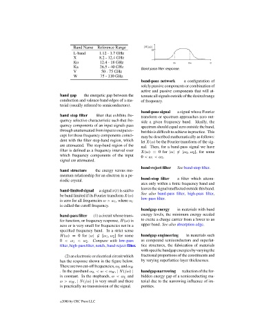
band-pass filter (1) a circuit whose trans- energy levels, the minimum energy needed
fer function, or frequency response, H(ω) is to excite a charge carrier from a lower to an
zero or is very small for frequencies not in a upper band. See also absorption edge.
specified frequency band. In a strict sense
H(ω) = 0 for |ω|6∈[ω 1 ,ω 2 ] for some bandgap engineering in materials such
0 <ω 1 <ω 2 . Compare with low-pass as compound semiconductors and superlat-
filter, high-passfilter, notch, band-reject filter. tice structures, the fabrication of materials
with specific bandgap energies by varying the
(2) an electronic or electrical circuit which fractional proportions of the constituents and
has the response shown in the figure below. by varying superlattice layer thicknesses.
Therearetwocut-offfrequencies, ω L andω H
. In the passband ω L <ω <ω H , | N(jω) | bandgap narrowing reduction of the for-
is constant. In the stopbands, ω< ω L and bidden energy gap of a semiconducting ma-
ω> ω H , | N(jω) | is very small and there terial due to the narrowing influence of im-
is practically no transmission of the signal. purities.
c
2000 by CRC Press LLC