
Page 290 - Fundamentals of Light Microscopy and Electronic Imaging
P. 290
IMAGING PERFORMANCE OF A CCD DETECTOR 273
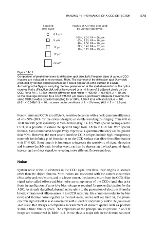
Selected Radius of Airy disk produced
pixel sizes by various objectives
6.8 m
100×, 1.30 NA = 26 m
9 m 63×, 1.25 NA = 16 m
40×, 1.30 NA = 10 m
32×, 0.40 NA = 27 m
12 m
10×, 0.25 NA = 13 m
17 m
23 m
Figure 14-11
Comparison of pixel dimensions to diffraction spot size. Left: The pixel sizes of various CCD
imagers are indicated in micrometers. Right: The diameter of the diffraction spot (Airy disk)
produced by various objective lenses as it would appear on a the surface of a CCD.
According to the Nyquist sampling theorm, preservation of the spatial resolution of the optics
requires that a diffraction disk radius be covered by a minimum of 2 adjacent pixels on the
CCD. For a 40 , 1.3 NA lens the diffraction spot radius 40(0.61 0.546)/1.3 10 m,
so the coverage provided by a CCD with 6.8 m pixels is just barely adequate. However, the
same CCD provides excellent sampling for a 100 , 1.3 NA lens with spot radius 100
(0.61 0.546)/1.3 26 m, even under conditions of 2 2 binning (6.8 2 13.6 m).
front-illuminated CCDs are efficient, sensitive detectors with a peak quantum efficiency
of 40–50% (80% for the newest designs) at visible wavelengths ranging from 400 to
1100 nm with peak sensitivity at 550–800 nm (Fig. 14-12). With special coatings on the
CCD, it is possible to extend the spectral range from 120 to 1100 nm. With special
thinned, back-illuminated designs (very expensive!), quantum efficiency can be greater
than 90%. However, the most recent interline CCD designs include high-transparency
materials for defining pixel boundaries on the CCD surface that allow front illumination
with 80% QE. Sometimes it is important to increase the sensitivity of signal detection
and improve the S/N ratio in other ways, such as by decreasing the background signal,
increasing the object signal, or selecting more efficient fluorescent dyes.
Noise
System noise refers to electrons in the CCD signal that have their origins in sources
other than the object photons. Most noises are associated with the camera electronics
(bias noise and read noise), and to a lesser extent, the thermal noise from the CCD. Bias
signal (also called offset) and bias noise are components of the CCD signal that arise
from the application of a positive bias voltage as required for proper digitization by the
ADC. As already described, thermal noise refers to the generation of electrons from the
kinetic vibrations of silicon atoms in the CCD substrate. It is common to refer to the bias
noise and thermal noise together as the dark noise. As we will see later on, the photo-
electron signal itself is also associated with a level of uncertainty called the photon or
shot noise that always accompanies measurement of discrete quanta such as photons
within a finite time or space. The amplitudes of the principal noises present in a CCD
image are summarized in Table 14-1. Noise plays a major role in the determination of