
Page 323 - MEMS and Microstructures in Aerospace Applications
P. 323
Osiander / MEMS and microstructures in Aerospace applications DK3181_c014 Final Proof page 317 1.9.2005 12:47pm
Material Selection for Applications of MEMS 317
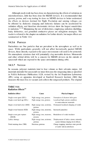
Although much work has been done on characterizing the effects of radiation on
microelectronics, little has been done for MEMS devices. It is recommended that
gamma, proton, and x-ray testing be done on MEMS devices to better understand
the effects on devices destined for flight. Excitation and sensing voltages can
be effected by dielectric charging and dielectric failures can be accelerated by
radiation effects, and therefore electrostatic devices show the largest sensitivities
to radiation. 21–24 Minimizing the use of dielectrics, employing radiation shielding,
leaky dielectrics, and grounded conductive planes are mitigation strategies. The
reader is referred to the chapter on radiation for further details, but major effects are
summarized in Table 14.6.
14.5.6 PARTICLES
Particulates are fine particles that are prevalent in the atmosphere as well as in
space. While particulates generally will not affect hermetically packed MEMS
devices, those directly exposed to the space environment will need to be protected.
On atmospheric missions dust will potentially clog moveable devices. Meteoroids
and other orbital debris will be a concern for MEMS devices on the outside of
spacecraft which are exposed to the space environment during orbit.
14.5.7 VACUUM
In vacuum, polymer materials tend to lose volume as their solvents outgas. All
materials intended for spacecraft use must first pass the outgassing data as specified
in NASA Reference Publication 1124, revised by the Jet Propulsion Laboratory
(JPL) using an apparatus developed at Stanford Research Institute (SRI) that
measures the mass loss in vacuum and collects the outgassed products. The original
TABLE 14.6
Radiation Effects 33
Radiation Effect Cause Physical Impact
Single event upset (SEU) High energy ions, protons Formation of electron–hole pairs
Single event latch-up (SEL) High energy ions, protons Localized high current condition
in semiconductor materials
Single event hard error (SHE) High energy ions, neutrons, Permanent localized charging of oxide
protons
Single event burnout (SEB) High energy ions, neutrons, Increased parasitics
protons
Single event gate rupture High energy ions, neutrons, Breakdown of oxide insulator
(SEGR) protons
Lattice damage High energy ions, neutrons, Displacement of lattice atoms; minority
protons carrier lifetime doping level effects
Total ionizing dose (TID) Electrons, protons Charge trapping, interface state growth
at oxide–silicon interfaces
© 2006 by Taylor & Francis Group, LLC