
Page 83 -
P. 83
3-38 MEMS: Design and Fabrication
sink. Its thermal expansion coefficient is closely matched to Pyrex® glass but exhibits considerable tem-
perature dependence. A good match in thermal expansion coefficient between the device wafer and the
support substrate is required. A poor match introduces stress, which degrades the device performance.
This makes it difficult to fabricate composite structures of Pyrex® and Si that are stress-free over a wide
range of temperatures. Drift in silicon sensors often stems from packaging. In this respect, several types
of stress-relief (subassemblies for stress-free mounting of the active silicon parts) play a major role; using
silicon as the support for silicon sensors is highly desirable. Anodic bonding of Pyrex® glass to Si in this
respect is inferior to fusion bonding of SitoSi [Shimbo et al., 1986; Tong et al., 1994; Barth, 1990].
Although the Si band gap is relatively narrow, by employing silicon-on-insulator (SOI) wafers (see
Section 3.18.1), high-temperature sensors can be fashioned. For the latter application, relatively highly
doped Si, which is relatively linear in its temperature coefficient of resistance and sensitivity over a wide
range, typically is employed.
When fabricating thermally isolated structures on Si, the large thermal conductivity of Si poses a con-
siderable problem, as the major heat leak occurs through the Si material. For thermally isolated struc-
tures, machining in glass, quartz, or ceramics, with their lower thermal conductivity, represents an
important alternative.
3.6.2 Silicon Optical Properties
Silicon features an indirect band gap and is not an active optical material. As a consequence, silicon-based
lasers do not exist. Silicon is effective only in detecting light as the indirect band gap makes emission of
light difficult. Above 1.1 µm, silicon is transparent, but at wavelengths shorter than 0.4µm (in the blue
and ultraviolet portions of the visible spectrum), it reflects over 60% of the incident light. One of the
most established applications for silicon sensors, although not often typified as MEMS, is visual imaging
with charge-coupled devices (CCDs). In a CCD imager, each element in a two-dimensional array gener-
ates an electrical charge in proportion to the amount of light it receives. The charge, stored by CCD ele-
ments along a row, is subsequently transferred to the next element in bucket-brigade fashion as the light
input is read out line by line. The number of picture elements (pixels) on the CCD determines the reso-
lution. In the top-of-the-line CCD cameras ( http://www.pctechguide.com/19digcam.htm ), a 3.34
megapixel CCD is capable of delivering a maximum image size of 2048 1536 pixels. Si as the pixel
semiconductor can be used for a wide variety of electromagnetic radiation wavelengths, from gamma rays
to infrared. There is a trend now to configure pixels in clever ways to make novel optical sensors feasible.
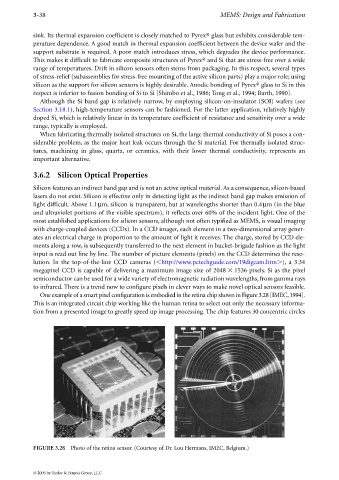
One example of a smart pixel configuration is embodied in the retina chip shown in Figure 3.28 [IMEC,1994].
This is an integrated circuit chip working like the human retina to select out only the necessary informa-
tion from a presented image to greatly speed up image processing. The chip features 30 concentric circles
FIGURE 3.28 Photo of the retina sensor. (Courtesy of Dr. Lou Hermans, IMEC, Belgium.)
© 2006 by Taylor & Francis Group, LLC