
Page 233 - A Practical Guide from Design Planning to Manufacturing
P. 233
Circuit Design 205
Instead, research is focusing on new high-K materials that will increase
the oxide permittivity. Charge mobility is improved by strained silicon
processes, which either push the silicon atoms in PMOS channels closer
together or pull the atoms in NMOS channels apart. For all silicon
MOSFETs, the mobility of holes in PMOS devices is only about half the
mobility of electrons in NMOS devices. The movement of holes is caused
by the movement of electrons in the opposite direction, but because
many different electrons are involved in moving a single hole, the process
is much less efficient than NMOS devices where each charge carrier is
a single free electron. To make up for the difference in mobility, circuit
designers routinely make the width of PMOS devices double the width
of NMOS devices.
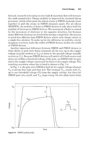
Another important difference between NMOS and PMOS devices is
their ability to pull their drain terminals all the way up to the supply
voltage (usually written as V ) or down to the ground voltage (usually
dd
written as V ). Because NMOS devices will switch off if both source and
ss
drain are within a threshold voltage of the gate, an NMOS with its gate
tied to the supply voltage cannot pull its drain to the supply voltage. The
resulting waveform when this is tried is shown in Fig. 7-4.
In Fig. 7-4, the gate of an NMOS is held at the supply voltage whereas
V is driven first high and then low. The terminal V out tracks with V in
in
up to one threshold voltage (V ) from the supply voltage, but then the
t
NMOS goes into cutoff, and V out stops rising. On the other hand when
V dd
V t
V out
V dd
Voltage V in
V in V out
V ss
Time
Figure 7-4 NMOS pulling high.