
Page 239 - A Practical Guide from Design Planning to Manufacturing
P. 239
Circuit Design 211
is blocked from the output by the off P-device and the signal on N-device
pulls the output to a 0. The final case at the bottom right shows both
inputs high and both N-devices pulling the output to a 0.
CMOS logic gates always include one network of transistors to pull
the output down and another to pull the output up. The networks are
designed, so that they are never both be on at the same time. NMOS
transistors are used for the pulldown network because they are effec-
tive at driving low voltages. PMOS transistors are used for the pullup
network because they are effective at driving high voltages. The result
is that CMOS logic gates are always inverting. A rising input will turn
on an NMOS and turn off a PMOS, which will either cause the gate
output to go low or stay the same. A falling input will turn on a PMOS
and turn off an NMOS, which will either cause the gate output to go high
or stay the same. Arising input never causes a rising output, and a falling
input never causes a falling output. To make noninverting logic like an
AND, CMOS logic uses an inverting gate like an NAND followed by an
inverter.
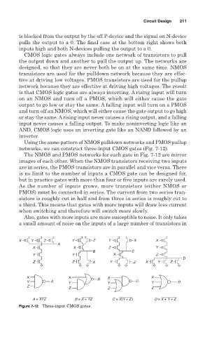
Using the same pattern of NMOS pulldown networks and PMOS pullup
networks, we can construct three-input CMOS gates (Fig. 7-12).
The NMOS and PMOS networks for each gate in Fig. 7-12 are mirror
images of each other. When the NMOS transistors receiving two inputs
are in series, the PMOS transistors are in parallel and vice versa. There
is no limit to the number of inputs a CMOS gate can be designed for,
but in practice gates with more than four or five inputs are rarely used.
As the number of inputs grows, more transistors (either NMOS or
PMOS) must be connected in series. The current from two series tran-
sistors is roughly cut in half and from three in series is roughly cut to
a third. This means that gates with more inputs will draw less current
when switching and therefore will switch more slowly.
Also, gates with more inputs are more susceptible to noise. It only takes
a small amount of noise on the inputs of a large number of transistors in
X Y Z Y Z Y X X
A
X X Z Y
B C
Y Y X Z
D
Z Z X Y Z X Y Z
X X B X X
Y A Y Y C Y D
Z
Z Z Z
A = XYZ B = X + YZ C = X(Y + Z) D = X + Y + Z
Figure 7-12 Three-input CMOS gates.