
Page 88 - A Practical Guide from Design Planning to Manufacturing
P. 88
64 Chapter Two
into registers. The register file is implemented as a section of transis-
tors at the heart of the microprocessor die. Its small size and physical
location directly next to the portion of the die performing calculations
are what make its very low latencies possible. The effective cost of this
die area is extremely high because increasing the capacity of the regis-
ter file will push the other parts of the die farther apart, possibly lim-
iting the maximum processor frequency. Also the latency of the register
file will increase if its capacity is increased.
Making any memory store larger will always increase its access time.
So the register file is typically kept small to allow it to provide laten-
cies of only a few processor cycles; but operating at billions of calcula-
tions per second, it won’t be long before the processor will need a piece
of data not in the register file. The first place the processor looks next
for data is called cache memory.
Cache memory is high-speed memory built into the processor die. It
has higher capacity than the register file but a longer latency. Cache
memories reduce the effective memory latency by storing data that has
recently been used. If the processor accesses a particular memory loca-
tion while running a program, it is likely to access it more than once.
Nearby memory locations are also likely to be needed.
By loading and storing memory values and their neighboring locations
as they are accessed, cache memory will often contain the data the
processor needs. If the needed data is not found in the cache, it will have
to be retrieved from the next level of the memory hierarchy, the com-
puter’s main memory. The percentage of time the needed data is found
when the cache is accessed is called the hit rate. A larger cache will pro-
vide a higher hit rate but will also take up more die area, increasing the
processor cost. In addition, the larger the cache capacity, the longer its
latency will be. Table 2-10 shows some of the trade-offs in designing
cache memory.
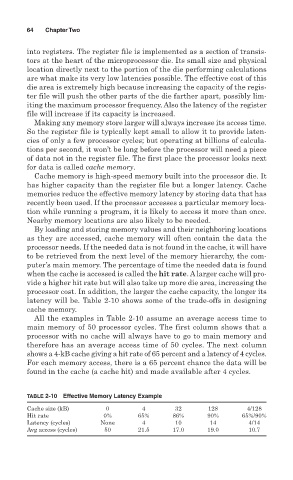
All the examples in Table 2-10 assume an average access time to
main memory of 50 processor cycles. The first column shows that a
processor with no cache will always have to go to main memory and
therefore has an average access time of 50 cycles. The next column
shows a 4-kB cache giving a hit rate of 65 percent and a latency of 4 cycles.
For each memory access, there is a 65 percent chance the data will be
found in the cache (a cache hit) and made available after 4 cycles.
TABLE 2-10 Effective Memory Latency Example
Cache size (kB) 0 4 32 128 4/128
Hit rate 0% 65% 86% 90% 65%/90%
Latency (cycles) None 4 10 14 4/14
Avg access (cycles) 50 21.5 17.0 19.0 10.7