
Page 105 - A Practical Guide from Design Planning to Manufacturing
P. 105
80 Chapter Three
48
Si
debug
36 debug
Design time (months) 24 debug Physical Physical
Si
design
Si
design
design
12 Physical Behavioral
Behavioral design
design
Behavioral
Si design Design
Design
debug Spec spec spec
0
Repackage Compaction or Proliferation Lead
variation
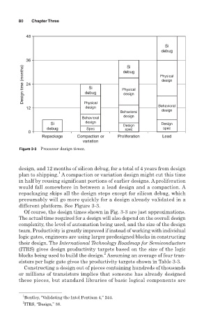
Figure 3-3 Processor design times.
design, and 12 months of silicon debug, for a total of 4 years from design
1
plan to shipping. A compaction or variation design might cut this time
in half by reusing significant portions of earlier designs. A proliferation
would fall somewhere in between a lead design and a compaction. A
repackaging skips all the design steps except for silicon debug, which
presumably will go more quickly for a design already validated in a
different platform. See Figure 3-3.
Of course, the design times shown in Fig. 3-3 are just approximations.
The actual time required for a design will also depend on the overall design
complexity, the level of automation being used, and the size of the design
team. Productivity is greatly improved if instead of working with individual
logic gates, engineers are using larger predesigned blocks in constructing
their design. The International Technology Roadmap for Semiconductors
(ITRS) gives design productivity targets based on the size of the logic
2
blocks being used to build the design. Assuming an average of four tran-
sistors per logic gate gives the productivity targets shown in Table 3-3.
Constructing a design out of pieces containing hundreds of thousands
or millions of transistors implies that someone has already designed
these pieces, but standard libraries of basic logical components are
1
Bentley, “Validating the Intel Pentium 4,” 244.
2
ITRS, “Design,” 38.