
Page 37 - A Practical Guide from Design Planning to Manufacturing
P. 37
The Evolution of the Microprocessor 13
altogether. The courts could easily decide for either side. Rather than
pursue total victory at the risk of total destruction, in 1966, both compa-
nies agreed to cross license their patents to each other. They also agreed
to sell licenses for both patents for a small percentage of the profits, to
anyone else who wanted to make integrated circuits. When later court
cases found first in favor of Kilby and then in favor of Noyce, it no longer
mattered, and today they are considered coinventors of the integrated
circuit.
In 1960, Bell Labs made another key advance, creating the first suc-
cessful field-effect transistor. This was the same transistor that Shockley
had originally set out to build 15 years earlier and Lilienfeld had first
proposed 15 years before that, but no one had been able to make it
work. The key turned out to be the same silicon dioxide layer that Noyce
had proposed using. A group headed by John Atalla showed that by
carefully cleaning the silicon surface and then growing an oxide layer
the surface states could be eliminated. The electric field from a metal
wire deposited on top of the oxide could penetrate the silicon and turn
on and off a flow of current. Because it was a vertical stack of metal,
oxide, and semiconductor, this device was named the Metal Oxide
Semiconductor Field-Effect Transistor (MOSFET).
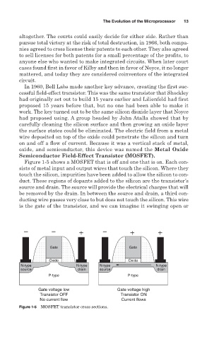
Figure 1-5 shows a MOSFET that is off and one that is on. Each con-
sists of metal input and output wires that touch the silicon. Where they
touch the silicon, impurities have been added to allow the silicon to con-
duct. These regions of dopants added to the silicon are the transistor’s
source and drain. The source will provide the electrical charges that will
be removed by the drain. In between the source and drain, a third con-
ducting wire passes very close to but does not touch the silicon. This wire
is the gate of the transistor, and we can imagine it swinging open or
− − + − + +
Gate Gate
Oxide Oxide
N-type N-type N-type N-type
source drain source drain
P-type P-type
Gate voltage low Gate voltage high
Transistor OFF Transistor ON
No current flow Current flows
Figure 1-5 MOSFET transistor cross sections.