
Page 12 - Nanotechnology an introduction
P. 12
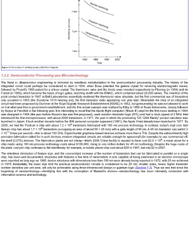
Figure 1.2 The evolution of machining accuracy (after Norio Taniguchi).

  1.3.2. Semiconductor Processing qua Microtechnology

  The  trend  in  ultraprecision  engineering  is  mirrored  by  relentless  miniaturization  in  the  semiconductor  processing  industry.  The  history  of  the
  integrated circuit could perhaps be considered to start in 1904, when Bose patented the galena crystal for receiving electromagnetic waves,
  followed by Picard's 1906 patent for a silicon crystal. The thermionic valve and the triode were invented respectively by Fleming (in 1904) and de
  Forest (in 1906), which became the basis of logic gates, reaching zenith with the ENIAC, which contained about 20,000 valves. The invention of the
  point contact transistor in 1947 at Bell Laboratories essentially rendered the thermionic valve obsolete, but the first commercial use of transistors
  only occurred in 1953 (the Sonotone 1010 hearing aid), the first transistor radio appearing one year later. Meanwhile the idea of an integrated
  circuit had been proposed by Dummer at the Royal Signals Research Establishment (RSRE) in 1952, but (presumably) he was not allowed to work
  on it at what was then a government establishment, and the first actual example was realized by Kilby in 1958 at Texas Instruments, closely followed
  by Noyce at Fairchild in the following year. It is interesting to recall that the Apollo flight computer (“Block II”) used for the first moon landing in 1969
  was designed in 1964 (the year before Moore's law was first proposed), used resistor–transistor logic (RTL) and had a clock speed of 2 MHz. Intel
  introduced the first microprocessor, with about 2000 transistors, in 1971, the year in which the pioneering “LE-120A Handy” pocket calculator was
  launched in Japan. It took another decade before the IBM personal computer appeared (1981); the Apple II had already been launched in 1977. By
                                               6
  2000, we had the Pentium 4 chip with about 1.2 × 10  transistors fabricated with 180 nm process technology. In contrast, today's dual core Intel
                            9
  Itanium chip has about 1.7 × 10  transistors (occupying an area of about 50 × 20 mm) with a gate length of 90 nm. A 45 nm transistor can switch 3
     11
  × 10  times per second—this is about 100 GHz. Experimental graphene-based devices achieve more than a THz. Despite the extraordinarily high
  precision fabrication called for in such devices, modern integrated circuits are reliable enough for spacecraft (for example) to use commercial off-
                                                                                                         9
  the-shelf (COTS) devices. The fabrication plants are not cheap—Intel's 2008 China facility is reputed to have cost $2.5 × 10 : a mask alone for a
  chip made using 180 nm process technology costs about $100,000, rising to one million dollars for 45 nm technology. Despite the huge costs of
  the plant, cost per chip continues to fall relentlessly: for example, a mobile phone chip cost about $20 in 1997, but only $2 in 2007.
  The relentless diminution of feature size, and the concomitant increase of the number of transistors that can be fabricated in parallel on a single
  chip, has been well documented; structures with features a few tens of nanometers in size capable of being examined in an electron microscope
  were reported as long ago as 1960; device structures with dimensions less than 100 nm were already being reported in 1972, with 25 nm achieved
  in 1979. Incidentally, the lower size limit for practical semiconductor circuits is considered to be 20 nm; smaller sizes, hence higher transistor
  number densities per unit area, will only be achievable using three-dimensional design or quantum logic (Section 7.3). Thus we see that since the
  beginning  of  nanotechnology—identifying  this  with  the  conception  of  Maxwell's  demon—nanotechnology  has  been  intimately  connected  with
  information science and technology.