
Page 21 - Nanotechnology an introduction
P. 21
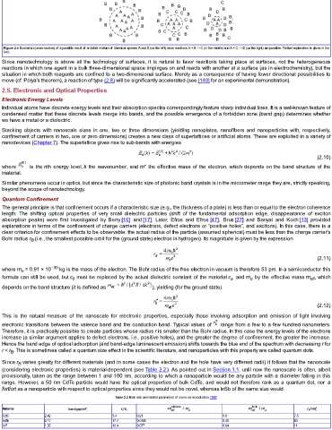
Figure 2.4 Illustration (cross-section) of a possible result of an initial mixture of chemical species A and B (on the left) when reactions A + B → C (in the middle) and A + C → D (on the right) are possible. Further explanation is given in the
  text.
  Since nanotechnology is above all the technology of surfaces, it is natural to favor reactions taking place at surfaces, not the heterogeneous
  reactions in which one agent in a bulk three-dimensional space impinges on and reacts with another at a surface (as in electrochemistry), but the
  situation in which both reagents are confined to a two-dimensional surface. Merely as a consequence of having fewer directional possibilities to
  move (cf. Pólya's theorem), a reaction of type (2.8) will be significantly accelerated (see [140] for an experimental demonstration).
  2.5. Electronic and Optical Properties
  Electronic Energy Levels
  Individual atoms have discrete energy levels and their absorption spectra correspondingly feature sharp individual lines. It is a well-known feature of
  condensed matter that these discrete levels merge into bands, and the possible emergence of a forbidden zone (band gap) determines whether
  we have a metal or a dielectric.

  Stacking objects with nanoscale sizes in one, two or three dimensions (yielding nanoplates, nanofibers and nanoparticles with, respectively,
  confinement of carriers in two, one or zero dimensions) creates a new class of superlattices or artificial atoms. These are exploited in a variety of
  nanodevices (Chapter 7). The superlattice gives rise to sub-bands with energies


                                                                                                                      (2.10)
  where      is  the nth  energy  level, k the wavenumber, and m* the effective mass of the electron, which depends on the band structure of the
  material.

  Similar phenomena occur in optics, but since the characteristic size of photonic band crystals is in the micrometer range they are, strictly speaking,
  beyond the scope of nanotechnology.
  Quantum Confinement
  The general principle is that confinement occurs if a characteristic size (e.g., the thickness of a plate) is less than or equal to the electron coherence
  length.  The  shifting  optical  properties  of  very  small  dielectric  particles  (shift  of  the  fundamental  adsorption  edge,  disappearance  of  exciton
  absorption  peaks)  were  first  investigated  by  Berry [16]  and [17].  Later,  Efros  and  Efros [47],  Brus [27]  and  Banyai  and  Koch [13]  provided
  explanations in terms of the confinement of charge carriers (electrons, defect electrons or “positive holes”, and excitons). In this case, there is a
  clear criterion for confinement effects to be observable: the actual radius of the particle (assumed spherical) must be less than the charge carrier's
  Bohr radius r  (i.e., the smallest possible orbit for the (ground state) electron in hydrogen). Its magnitude is given by the expression
            B


                                                                                                                      (2.11)

  where m  = 0.91 × 10 −30  kg is the mass of the electron. The Bohr radius of the free electron in vacuum is therefore 53 pm. In a semiconductor this
         e
  formula can still be used, but ϵ  must be replaced by the actual dielectric constant of the material ϵ , and m  by the effective mass m , which
                            0
                                                                                      s
                                                                                                                   eff
                                                                                             e
  depends on the band structure (it is defined as        ), yielding (for the ground state)
                                                                                                                      (2.12)
  This  is  the  natural  measure  of  the  nanoscale  for  electronic  properties,  especially  those  involving  adsorption  and  emission  of  light  involving
  electronic transitions between the valence band and the conduction band. Typical values of   range from a few to a few hundred nanometers.
  Therefore, it is practically possible to create particles whose radius r is smaller than the Bohr radius. In this case the energy levels of the electrons
  increase (a similar argument applies to defect electrons, i.e., positive holes), and the greater the degree of confinement, the greater the increase.
  Hence the band edge of optical adsorption (and band-edge luminescent emission) shifts towards the blue end of the spectrum with decreasing r for
  r < r . This is sometimes called a quantum size effect in the scientific literature, and nanoparticles with this property are called quantum dots.
     B
  Since r  varies greatly for different materials (and in some cases the electron and the hole have very different radii) it follows that the nanoscale
        B
  (considering electronic properties) is material-dependent (see Table 2.2). As pointed out in Section 1.1, until now the nanoscale is often, albeit
  provisionally, taken as the range between 1 and 100 nm, according to which a nanoparticle would be any particle with a diameter falling in this
  range. However, a 50 nm CdTe particle would have the optical properties of bulk CdTe, and would not therefore rank as a quantum dot, nor  a
  fortiori as a nanoparticle with respect to optical properties since they would not be novel, whereas InSb of the same size would.
                                           Table 2.2 Bohr radii and related parameters of some semiconductors [158]

  Material                bandgap/eV a        ϵ s /ϵ 0                                                            r B /nm b
  CdS            2.42                     5.4      0.21                            0.8                       7.5
  InSb           0.17                     17.7     0.0145                          0.40                      60
  InP            1.35                     12.4     0.077                           0.64                      11