
Page 34 - Optofluidics Fundamentals, Devices, and Applications
P. 34
Basic Micr ofluidic and Soft Lithographic Techniques 15
High-resolution
Light transparency
Si
Photoresist
(a) Perform photolithography
Si Master
(b) Pour PDMS over master;
cure at 70°C for 1h
PDMS
Si
(c) Peel PDMS from master
PDMS
(d) Seal against a flat surface
Microchannel
PDMS
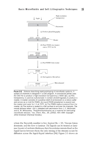
FIGURE 2-2 Scheme describing rapid prototyping of microfl uidic systems. A
system of channels is designed in a CAD program. A commercial printer uses
the CAD fi le to produce a high-resolution transparency (~5000 dpi). (a) This
transparency is used as a photomask in contact photolithography to produce a
master. A master consists of a positive relief of photoresist on a silicon wafer
and serves as a mold for PDMS. (b) Liquid PDMS prepolymer is poured over
the master and cured for 1 h at 70°C. (c) The PDMS replica is peeled from the
master. (d) The replica is sealed to a fl at surface to enclose the channels. The
overall process takes ~24 h. (Adapted with permission from J. C. McDonald
and G. M. Whitesides, “Poly(dimethylsiloxane) as a material for fabricating
microfluidic devices,” Acc. Chem. Res., 35, (2002), 491–499 . Copyright
2002 American Chemical Society.)
where the Reynolds number is low (typical Re < 10). Viscous forces
dominate, and the flow is laminar. The liquids can be treated as lami-
nae (layers) of uniform thickness; their boundaries remain fixed as the
liquid moves between them; the only mixing of the streams occurs by
diffusion across the liquid-liquid interface [36]. Figure 2-3 shows an