
Page 80 - Organic Electronics in Sensors and Biotechnology
P. 80
Or ganic Thin-Film Transistors for Inor ganic Substance Monitoring 57
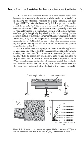
OTFTs are three-terminal devices in which charge conduction
between two terminals, the source and the drain, is controlled by
modulating the electrical potential of a third terminal, the gate.
A typical OTFT structure is shown in Fig. 2.1. The gate can be used to
switch the transistor “on” (high source-drain current) and “off” (negligible
source-drain current). The organic active layer is generally a few tens
of nanometers made of a conducting polymer or oligomer. The semi-
conducting film is typically deposited by solution processing (such as
solution casting, spin coating, Langmuir-Shäfer or Langmuir-Blodgett
techniques) or by thermal evaporation. The deposited thin films are
generally polycrystalline, to be more precise, films composed of con-
tiguous grains having size of few hundreds of nanometers (see the
magnification in Fig. 2.1).
In a simplified view, for a p-type semiconductor, the application
of a negative gate voltage leads to an accumulation of positive charge
carriers, and the thin film conductance increases (accumulation
mode), while the application of a positive gate voltage depletes the
major carriers and reduces the film conductance (depletion mode).
When enough charge carriers have been accumulated, the conducti-
vity increases dramatically, providing a conductive channel between
the source and drain electrodes. The typical I–V curves reported in
Organic semiconductor Conducting channel
⊕⊕⊕⊕⊕⊕⊕⊕⊕⊕⊕⊕⊕⊕⊕⊕⊕⊕⊕⊕
⊕⊕⊕⊕⊕⊕⊕⊕⊕⊕
Source ⊕⊕⊕⊕⊕⊕⊕⊕⊕⊕ Drain
SiO 2
I
Gate ds
V ds
V g
–60
E B
I ds (μA) –40
–20
0
0 –20 –40 –60 –80 –100
V (V)
g
FIGURE 2.1 Schematic structure of an organic thin-fi lm transistor (OTFT) with
a polycrystalline active layer and a typical I –V characteristic curves.
ds ds