
Page 81 - Organic Electronics in Sensors and Biotechnology
P. 81
58 Cha pte r T w o
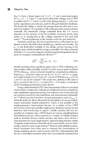
Fig. 2.1 show a linear region for V ≤ V – V and a saturation region
ds g t
for V > V – V . Here V is the device threshold voltage, that in TFTs
ds g t t
59
is equal to qNd/C , where N is the film doping density, C is the die-
i i
lectric capacitance per unit area, and d is the gate dielectric thickness.
The threshold voltage V marks the passage from the off to the on con-
t
ductivity regime. In transistors with undoped active semiconductor
60
materials, the threshold voltage extracted from the I–V curves
depends on the density of the low-mobility electronic levels (trap
states) as it corresponds to the voltage required to fill such trap
states, 61, 62 located primarily at the interface with the gate dielectric.
Generally speaking, the device performance is described by two
figures of merit: the field-effect mobility μ FET and the on/off ratio. The
μ is the field-effect mobility of the charge carriers moving in the
FET
organic layer, which should be as large as possible. It is often extracted
from the I–V curves by using the standard analytical equations devel-
oped for inorganic semiconductor devices 59, 63
W
⋅
I SAT = C μ ( V − V ) (2.1)
ds i g t
2 L
Strictly speaking, these equations apply only to TFTs exhibiting con-
stant charge carrier mobility, which is not the case for polycrystalline
OTFTs; thus μ values extracted should be considered as estimates.
FET
Typical μ FET extracted values are in the 10 to 10 cm /(V · s) range,
–1
–3
2
but values as high as 1 to 10 cm /(V · s) [a-Si:H TFTs have μ of 0.1 to
2
FET
1 cm /(V · s)] can be reached. The on/off ratio, defined as the ratio of
2
63
the I current in the on (V > V ) and off (V = 0 V) states, is indicative
ds g t g
of the switching performance of the device.
Using a three-terminal OTFT structure instead of the two-terminal
chemiresistor construction introduces additional process complexity
and complicates signal processing, but judicious use of the gate bias
can enhance sensitivity, discrimination, and measurement repeatabil-
ity. 64–68 Moreover, the extraction of many parameters such as μ , V ,
FET t
and bulk resistivity allows the partial deconvolution of various analyte-
sensor interaction related parameters, which is not possible in the
single-parameter chemiresistor devices. As a matter of fact, OTFT
devices have been successfully employed as chemical sensors for the
detection and monitoring of organic volatile analytes and less fre-
quently for inorganic ones. OTFTs based on various oligothiophenes
and phthalocyanines, when exposed to a variety of volatile analytes
such as alcohols, ketones, thiols, nitriles, and esters, have shown a
typical pattern for each single analyte, demonstrating that the variety
of organic semiconductor materials can be successfully used for fabri-
cating a selective array of gas sensors. More recently phthalocyanine-
58
based transistors have been used to measure the concentration of
strong oxidizing species, such as ozone and NO , demonstrating that
2
the use a field-effect transistor rather than conventional chemiresistors