
Page 68 - Photonics Essentials an introduction with experiments
P. 68
Electrical Response Time of Diodes
62 Photonic Devices
4.2 Modeling the Response Time of Photodiodes
The response time of a photodiode is determined by three different
factors:
1. The time required for minority carriers, created by the absorption
of a photon, to diffuse to the p-n junction
2. The time required for these carriers to drift across the depletion re-
gion
3. The time required for the external circuit to supply the necessary
majority carriers to balance the movement of minority carriers so
that charge neutrality is maintained
In almost every case, the response time will be determined by the
third factor. The rate at which the external circuit supplies the neces-
sary majority carriers is calculated from the capacitance of the photo-
diode and the series resistance of the circuit. The resistance–capaci-
tance (RC) charging time can be controlled to some degree, because
the capacitance of the diode depends on its bias voltage. The diffusion
and drift times are fixed by the conditions of diode fabrication.
In the following treatment, will evaluate each of these terms with
the objective of understanding their relative contributions. Some of
the results may appear to be counterintuitive. For example: the bias
voltage has very little effect on the intrinsic speed of response of a
photodiode. However, increasing the bias voltage will decrease the ca-
pacitance, and this has a significant effect on the extrinsic response
time. Efficient photodiodes can be made from direct band gap materi-
als as well as from indirect band gap materials. However, the intrin-
sic speed of response of indirect band gap photodiodes is lower be-
cause the photo-generated carriers are spread throughout a much
larger spatial extent of the device, and it takes more time to collect
them.
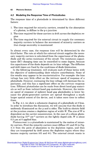
In Fig. 4.1, we show a schematic diagram of a photodiode at 0 bias.
In order to introduce the discussion, we will assume that the diode is
uniformly illuminated on the p and n sides. The built-in electric field
at the junction creates a depletion region of width W. The size of W is
dependent on the carrier concentration. In the case of a silicon photo-
diode having 10 16 cm –3 carriers on the lightly doped side, W is about
0.5 m at 0 applied bias.
Photocurrent in a photodiode is maintained by the motion of minor-
ity carriers. First the minority carriers must diffuse (#1 and #3 in Fig.
4.1) from the point of absorption to the depletion region, and then
they are transported by drift across the depletion region where they
become majority carriers (#2 and #4). The external circuit reacts to
Downloaded from Digital Engineering Library @ McGraw-Hill (www.digitalengineeringlibrary.com)
Copyright © 2004 The McGraw-Hill Companies. All rights reserved.
Any use is subject to the Terms of Use as given at the website.