
Page 73 - Photonics Essentials an introduction with experiments
P. 73
Electrical Response Time of Diodes
Electrical Response Time of Diodes 67
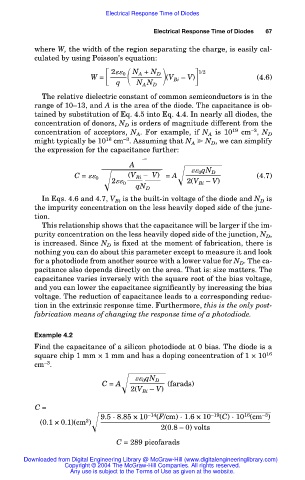
where W, the width of the region separating the charge, is easily cal-
culated by using Poisson’s equation:
2 0 N A + N D 1/2
W = (V Bi – V) (4.6)
q
N A N D
The relative dielectric constant of common semiconductors is in the
range of 10–13, and A is the area of the diode. The capacitance is ob-
tained by substitution of Eq. 4.5 into Eq. 4.4. In nearly all diodes, the
concentration of donors, N D is orders of magnitude different from the
concentration of acceptors, N A . For example, if N A is 10 19 cm , N D
–3
–3
might typically be 10 16 cm . Assuming that N A N D , we can simplify
the expression for the capacitance further:
A
0 qN D
q N 2(V Bi – V)
C = 0 (V Bi – V) = A (4.7)
2 0
D
In Eqs. 4.6 and 4.7, V Bi is the built-in voltage of the diode and N D is
the impurity concentration on the less heavily doped side of the junc-
tion.
This relationship shows that the capacitance will be larger if the im-
purity concentration on the less heavily doped side of the junction, N D ,
is increased. Since N D is fixed at the moment of fabrication, there is
nothing you can do about this parameter except to measure it and look
for a photodiode from another source with a lower value for N D . The ca-
pacitance also depends directly on the area. That is: size matters. The
capacitance varies inversely with the square root of the bias voltage,
and you can lower the capacitance significantly by increasing the bias
voltage. The reduction of capacitance leads to a corresponding reduc-
tion in the extrinsic response time. Furthermore, this is the only post-
fabrication means of changing the response time of a photodiode.
Example 4.2
Find the capacitance of a silicon photodiode at 0 bias. The diode is a
square chip 1 mm × 1 mm and has a doping concentration of 1 × 10 16
–3
cm .
0 qN D
C = A (farads)
2(V Bi – V)
C =
–14
16
–19
–3
(F/cm) · 1.6 × 10
(C)·10 (cm )
9.5 · 8.85 × 10
2
(0.1 × 0.1)(cm )
2(0.8 – 0) volts
C = 289 picofarads
Downloaded from Digital Engineering Library @ McGraw-Hill (www.digitalengineeringlibrary.com)
Copyright © 2004 The McGraw-Hill Companies. All rights reserved.
Any use is subject to the Terms of Use as given at the website.