
Page 75 - Photonics Essentials an introduction with experiments
P. 75
Electrical Response Time of Diodes
Electrical Response Time of Diodes 69
tion. This technique is widely used in both industry and the research
laboratory to characterize diodes for all kinds of applications. Such
measurements are shown in Figs. 4.4 and 4.5.
The time to charge the diode capacitance will depend on the resist-
ance in series with the diode. The intrinsic resistance of the diode will
depend inversely on its surface area. For most commercial photodi-
odes, this area tends to be large enough so that the series resistance
of the diode is negligibly small compared to the load resistance of the
measurement circuit. For a high-speed measurement, the input re-
sistance of the measurement circuit might be chosen to match the line
impedance of the coaxial cable or 50 . In this case, the RC time con-
stant of the diode in Example 4.2 would be 288 picofarads × 50 or
14,400 picoseconds. This is quite a bit longer than either the drift or
diffusion times discussed earlier. In most cases, you will find that the
time response of a photodiode will be limited by the RC time constant.
You can control this time constant over a range that is about a factor
of 2 by adjusting the reverse bias on the diode.
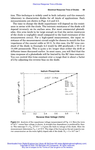
Figure 4.4. Analysis of the capacitance voltage measurement of Fig. 4.3. Here the term
2
2 –1
(C /A ) versus bias voltage is shown. A straight-line dependence is predicted by theo-
2
ry. The intercept V = V Bi , (C /A ) = 0 gives the built-in voltage of the diode. Here the
2 –1
measurement determines V Bi = +0.76 V. The slope of the line gives the net majority car-
rier concentration on the more lightly doped side of the diode: N D 5 × 10 16 cm .
–3
Downloaded from Digital Engineering Library @ McGraw-Hill (www.digitalengineeringlibrary.com)
Copyright © 2004 The McGraw-Hill Companies. All rights reserved.
Any use is subject to the Terms of Use as given at the website.