
Page 76 - Photonics Essentials an introduction with experiments
P. 76
Electrical Response Time of Diodes
70 Photonic Devices
pf –2
cm 4
(C/A) –2 , 10 –10
V B , Bias voltage
2
2 –1
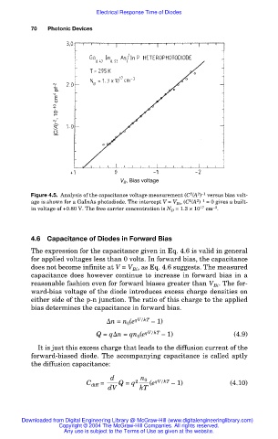
Figure 4.5. Analysis of the capacitance voltage measurement (C /A ) versus bias volt-
2
2 –1
age is shown for a GaInAs photodiode. The intercept V = V Bi , (C /A ) = 0 gives a built-
–3
in voltage of +0.80 V. The free carrier concentration is N D = 1.3 × 10 17 cm .
4.6 Capacitance of Diodes in Forward Bias
The expression for the capacitance given in Eq. 4.6 is valid in general
for applied voltages less than 0 volts. In forward bias, the capacitance
does not become infinite at V = V Bi , as Eq. 4.6 suggests. The measured
capacitance does however continue to increase in forward bias in a
reasonable fashion even for forward biases greater than V Bi . The for-
ward-bias voltage of the diode introduces excess charge densities on
either side of the p-n junction. The ratio of this charge to the applied
bias determines the capacitance in forward bias.
n = n 0 (e qV/kT – 1)
Q = q n = qn 0 (e qV/kT – 1) (4.9)
It is just this excess charge that leads to the diffusion current of the
forward-biased diode. The accompanying capacitance is called aptly
the diffusion capacitance:
d n 0
2
C diff = Q = q (e qV/kT – 1) (4.10)
dV kT
Downloaded from Digital Engineering Library @ McGraw-Hill (www.digitalengineeringlibrary.com)
Copyright © 2004 The McGraw-Hill Companies. All rights reserved.
Any use is subject to the Terms of Use as given at the website.