Page 432 - Power Electronics Handbook
P. 432
List  of  symbols   421
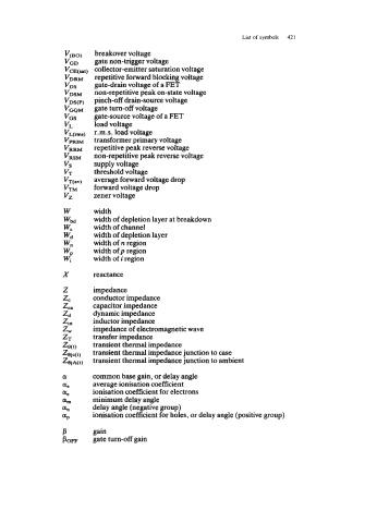
                           breakover voltage
                   V(BO)
                   VGD     gate non-trigger voltage
                   VCE(sat)   collector-emitter saturation voltage
                   VDRM    repetitive forward blocking voltage
                   vDS     gate-drain voltage of a FET
                   VDSM    non-repetitive peak on-state voltage
                   vDS(P)   pinch-off drain-source voltage
                   VGQM    gate turn-off voltage
                   vGS     gate-source voltage of a FET
                           load voltage
                           r.m.s. load voltage
                           transformer primary voltage
                           repetitive peak reverse voltage
                           non-repetitive peak reverse voltage
                           supply voltage
                           threshold voltage
                           average forward voltage drop
                           forward voltage drop
                           zener voltage

                           width
                           width of depletion layer at breakdown
                           width of channel
                           width of depletion layer
                           width of n region
                           width of p region
                           width of i region

                           reactance
                           impedance
                           conductor impedance
                           capacitor impedance
                           dynamic impedance
                           inductor impedance
                           impedance of electromagnetic wave
                           transfer impedance
                           transient thermal impedance
                           transient thermal impedance junction to case
                           transient thermal impedance junction to ambient
                           common base gain, or delay angle
                           average ionisation coefficient
                           ionisation coefficient for electrons
                           minimum delay angle
                           delay angle (negative group)
                           ionisation coefficient for holes, or delay angle (positive group)

                           gain
                           gate turn-off gain

