
Page 30 - Power Electronics Handbook
P. 30
Bipolar transistors 23
the high resistivity of the base material a good reverse characteristic is
obtained, and the n+ and p+ layers cause a large rate of carrier injection
into the high resistivity region, giving good forward characteristics.
Fast commutating rectifiers are often obtained using a double-diffused
construction. In this the starting material is high-resistivity n type, whicb is
chosen to withstand the required reverse voltage. Into this material n+ and
p+ diffusions are made, on opposite sides, for the cathode and anode
connections.
Even faster rectifiers are obtained using an e itaxial construction, as
shown in Figure 1.10. The base material is now n! Into this is grown an n
epitaxy layer of high resistivity, which is designed to provide the required
reverse voltage blocking capability. A p+ diffusion or ion implantation is
then made, to form the anode layer. This technique is capable of providing
devices in which the reverse recovery time rm is less than 100ns for a
component having a rating of over 1OOOV.
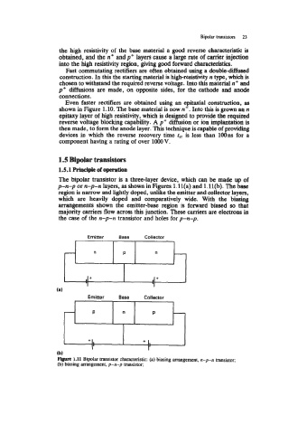
1.5 Bipolar transistors
1.5.1 Principle of opention
The bipolar transistor is a three-layer device, which can be made up of
p-n-p or n-p-n layers, as shown in Figures l.ll(a) and l.ll(b). The base
region is narrow and lightly doped, unlike the emitter and collector layers,
which are heavily doped and comparatively wide. With the biasing
arrangements shown the emitter-base region is forward biased so that
majority carriers flow across this junction. These carriers are electrons in
the case of the n-p-n transistor and holes for p-n-p.
7 n P n -
. I + I +
-
- P n P
- +I +I