
Page 25 - Power Electronics Handbook
P. 25
18 Power semiconductor devices
1.4 Power rectitfer operation
1.4.1 The diode curve
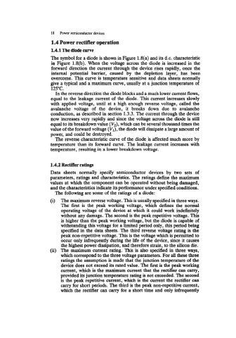
The symbol for a diode is shown in Figure 1.8(a) and its d.c. characteristic
in Figure 1.8(b). When the voltage across the diode is increased in the
forward direction the current through the device rises rapidly, once the
internal potential barrier, caused by the depletion layer, has been
overcome. This curve is temperature sensitive and data sheets normally
give a typical and a maximum curve, usually at a junction temperature oi
125°C.
In the reverse direction the diode blocks and a much lower current flows,
equal to the leakage current of the diode. This current increases slowly
with applied voltage, until at a high enough reverse voltage, called the
avalanche voltage of the device, it breaks down due to avalanche
conduction, as described in section 1.3.3. The current through the device
now increases very rapidly and since the voltage across the diode is still
equal to its breakdown value (Vz), which can be several thousand times the
value of the forward voltage (VI), the diode will dissipate a large amount of
power, and could be destroyed.
The reverse characteristic curve of the diode is affected much more by
temperature than its forward curve. The leakage current increases with
temperature, resulting in a lower breakdown voltage.
1.4.2 Rder ratings
Data sheets normally specify semiconductor devices by two sets of
parameters, ratings and characteristics. The ratings define the maximum
values at which the component can be operated without being damaged,
and the characteristics indicate its performance under specified conditions.
The following are some of the ratings of a diode:
The maximum reverse voltage. This is usually specified in three ways.
The first is the peak working voltage, which defines the normal
operating voltage of the device at which it could work indefinitely
without any damage. The second is the peak repetitive voltage. This
is higher than the peak working voltage, but the diode is capable of
withstanding this voltage for a limited period only, this period being
specified in the data sheets. The third reverse voltage rating is the
peak non-repetitive voltage. This is the voltage which is permitted to
occur only infrequently during the life of the device, since it causes
the highest power dissipation, and therefore strain, to the silicon die.
The maximum current rating. This is also specified in three ways,
which correspond to the three voltage parameters. For all these three
ratings the assumption is made that the junction temperature of the
device does not exceed its rated value. The first is the peak working
current, which is the maximum current that the rectifier can carry,
provided its junction temperature rating is not exceeded. The second
is the peak repetitive current, which is the current the rectifier can
carry for short periods. The thud is the peak non-repetitive current,
which the rectifier can carry for a short the and only infrequently