
Page 23 - Power Electronics Handbook
P. 23
16 Power semiconductor devices
3
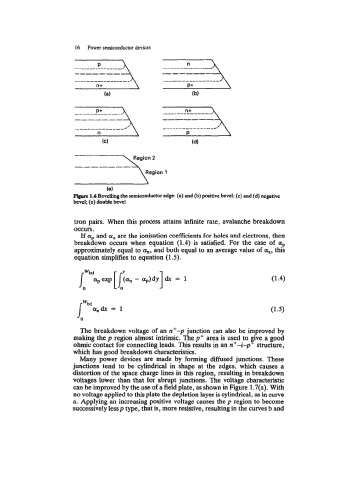
Region 2
-------
Region
1
(e)
1.6 Bevelling the semiconductor edge: (a) and (b) positive bevel; (c) and (d) negative
bevel; (e) double bevel
tron pairs. When this process attains infinite rate, avalanche breakdown
occurs.
If + and a, are the ionisation coefficients for holes and electrons, then
breakdown occurs when equation (1.4) is satisfied. For the case of a,,
approximately equal to q,, and both equal to an average value of a,, this
equation simplifies to equation (1 5).
The breakdown voltage of an n+-p junction can also be improved by
making the p region almost intrinsic. The p+ area is used to a good
ohmic contact for connecting leads. This results in an n+-i-p structure,
which has good breakdown characteristics.
Many power devices are made by forming diffused junctions. These
junctions tend to be cylindrical in shape at the edges, which causes a
distortion of the space charge lines in this region, resulting in breakdown
voltages lower than that for abrupt junctions. The voltage characteristic
can be improved by the use of a field plate, as shown in Figure 1.7(a). With
no voltage applied to this plate the depletion layer is cylindrical, as in curve
a. Applying an increasing positive voltage causes the p region to become
successively less p type, that is, more resistive, resulting in the curves b and