
Page 20 - Power Electronics Handbook
P. 20
Power recrifier principles 13
Depletion
l-=!--l I
I
+
n
\
'.
\
Pn
junction
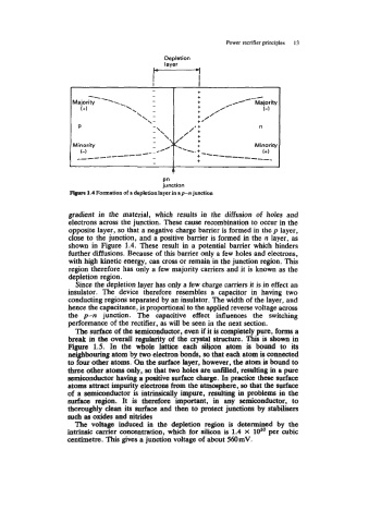
Figure 1.4 Formation of a depletion layer in ap-n junction
gradient in the material, which results in the diffusion of holes and
electrons across the junction. These cause recombination to occur in the
opposite layer, so that a negative charge barrier is formed in the p layer,
close to the junction, and a positive barrier is formed in the n layer, as
shown in Figure 1.4. These result in a potential barrier which hinders
further diffusions. Because of this barrier only a few holes and electrons,
with high kinetic energy, can cross or remain in the junction region. This
region therefore has only a few majority carriers and it is known as the
depletion region.
Since the depletion layer has only a few charge carriers it is in effect an
insulator. The device therefore resembles a capacitor in having two
conducting regions separated by an insulator. The width of the layer, and
hence the capacitance, is proportional to the applied reverse voltage across
the p-n junction. The capacitive effect influences the switching
performance of the rectifier, as will be seen in the next section.
The surface of the semiconductor, even if it is completely pure, forms a
break in the overall replarity of the crystal structure. This is shown in
Figure 1.5. In the whole lattice each silicon atom is bound to its
ncighbouring atom by two electron bonds, so that each atom is co~ecttd
to four other atoms. On tbe surface layer, however, the atom is bound to
three other atoms only, so that two holes are unfilled, resulting in a pure
semiconductor having a positive surface charge. In pr& these surface
atoms attract impurity electrons from the atmosphere, so that the surface
of a semiconductor is intrinsically impure, resulting in problems in the
surface region. It is therefore important, in any semiconductor, to
thoroughly clean its surface and then to protect junctions by stabilisers
such as oxides and nitrides
The voltage induced in the depletion region is determined by the
intrinsic carrier concentration, which for silicon is 1.4 x 10" per cubic
centimetre. This gives a junction voltage of about 560mV.